Vera Rubin Decoded Pt. 2 | Rubin GPU - Engineering Deep Dive
Where to Read What — Series Map
| Part | Title | Scope |
|---|---|---|
| 1 | Platform Framing & Architecture Map | Blackwell → Rubin platform thesis, headline specs |
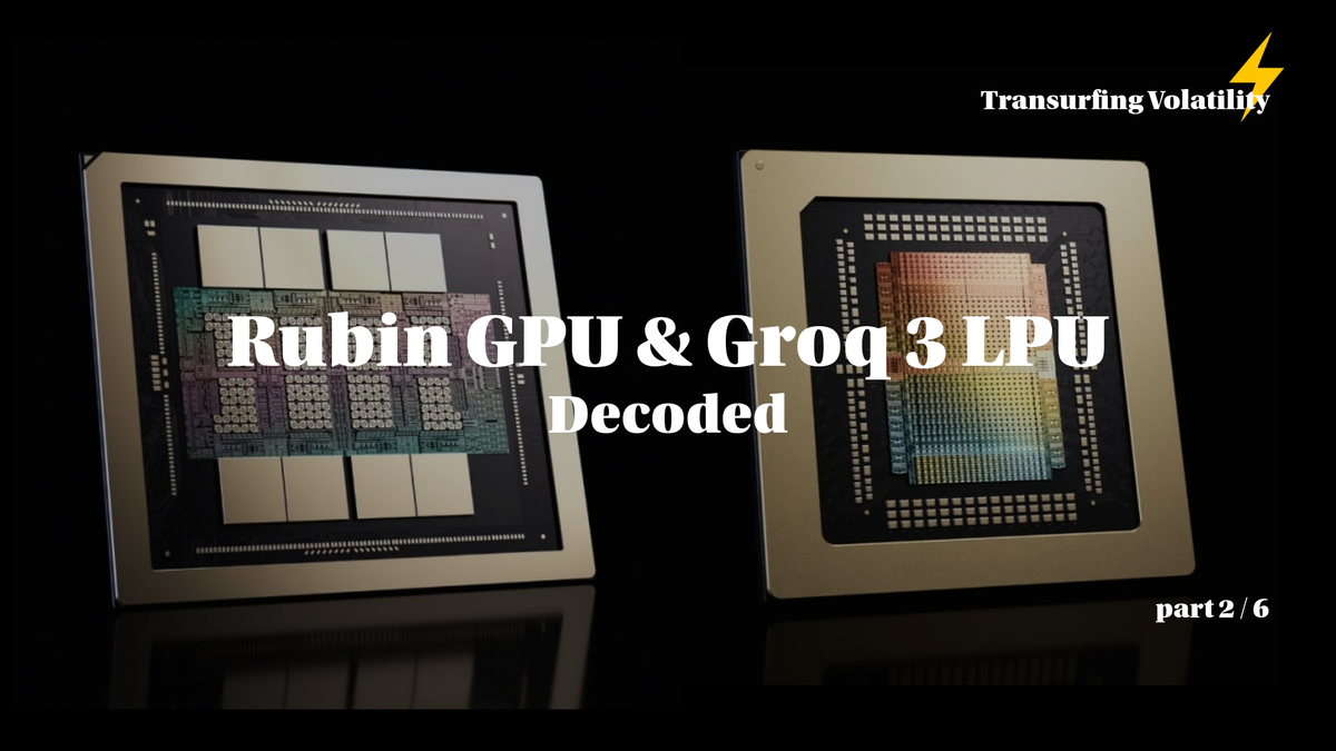
| 2 | Rubin GPU — Engineering Deep Dive (this part) | Process node, SMs, HBM4, NVLink-C2C, package, CPX + Groq 3 LPX |
| 3 | Vera CPU & the Networking Silicon Family | Vera CPU, NVLink 6 Switch, ConnectX-9, BlueField-4, Spectrum-6 |
| 4 | Rack Assembly — Trays, PCB, and Cooling | HGX vs NVL72, compute tray modules, cableless midplane, PCB upgrade, liquid cooling |
| 5 | Rack Power and the Networking Fabric | Power delivery, HVDC, tray↔rack wiring, scale-up NVLink 6, scale-out InfiniBand + Ethernet |
| 6 | Supply Chain — Master Reference | Suppliers by subsystem across the entire stack |
3. Rubin GPU — Engineering Deep Dive
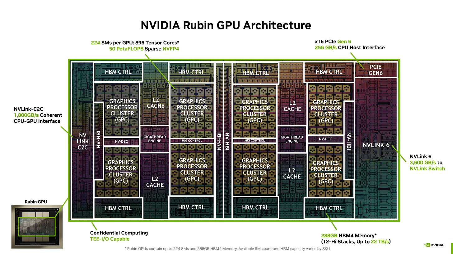
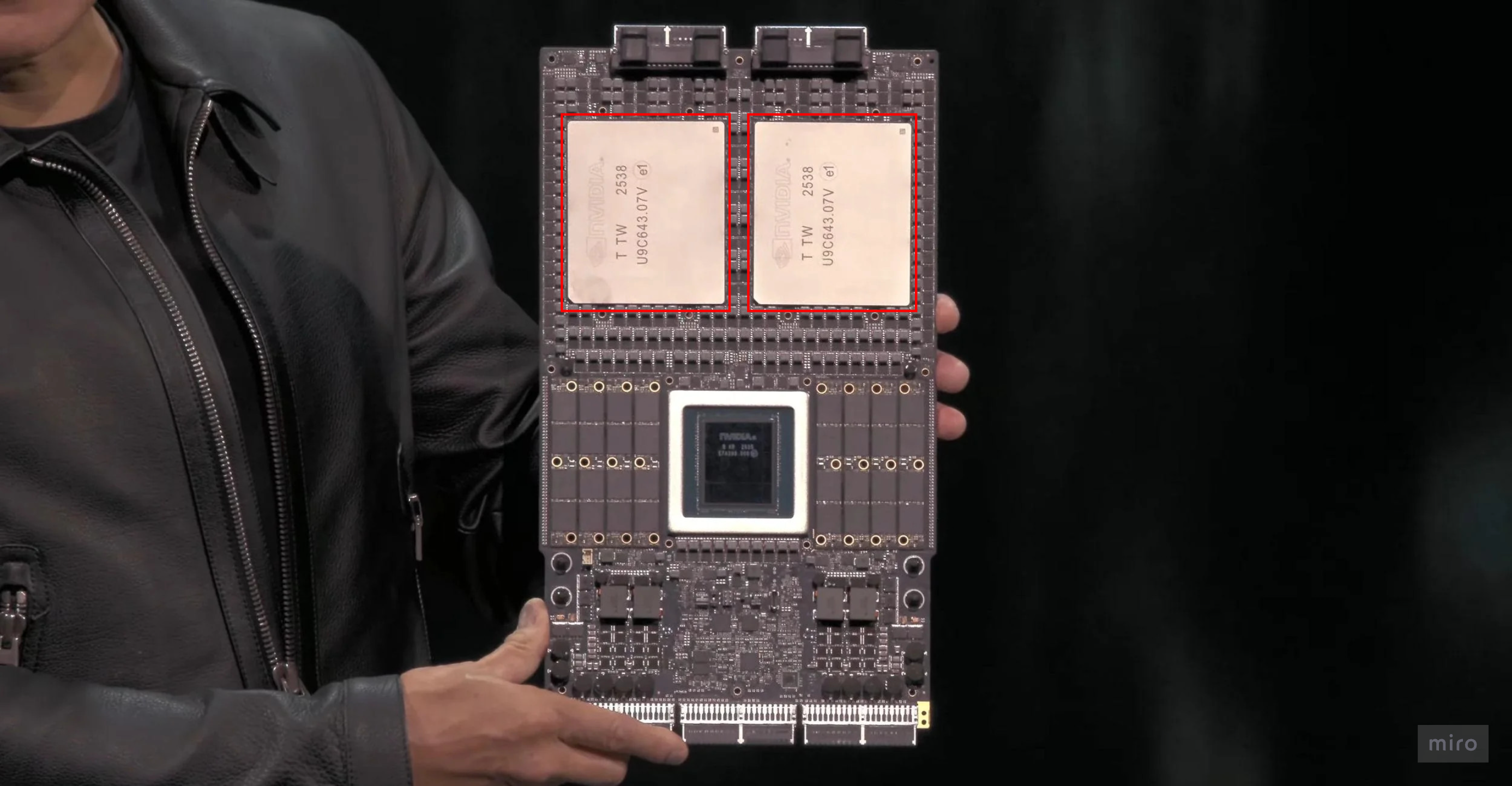
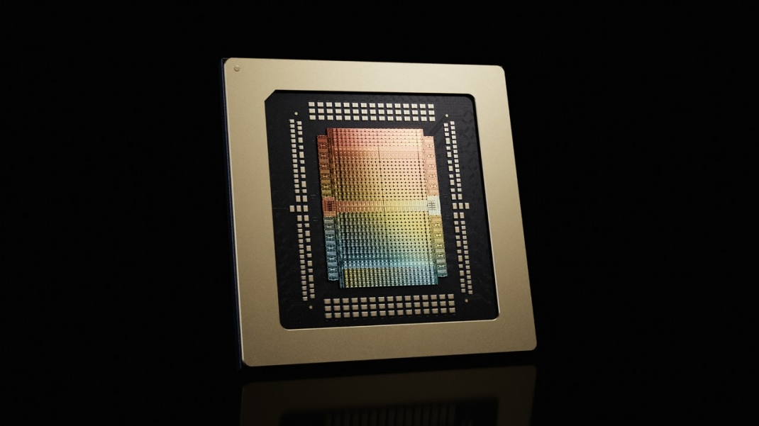
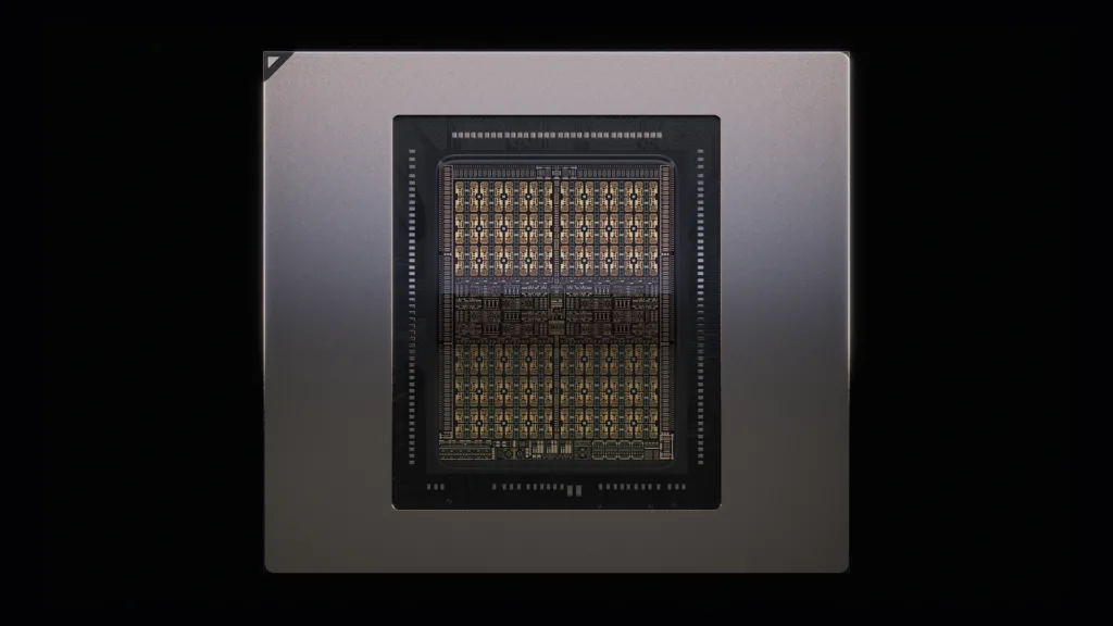
Rubin is a logical evolution of Blackwell, not a re-architecture. The basic structure stays the same: two reticle-sized logic dies side by side, each surrounded by HBM stacks. ("Reticle-sized" means each die is at the maximum size that current photolithography equipment can print in a single exposure — roughly 800 mm². A "die" is the actual square of silicon containing the chip's circuitry, before it is packaged.)
Eight HBM stacks sit alongside the two dies on the same package. The changes happen inside the dies and around the package.
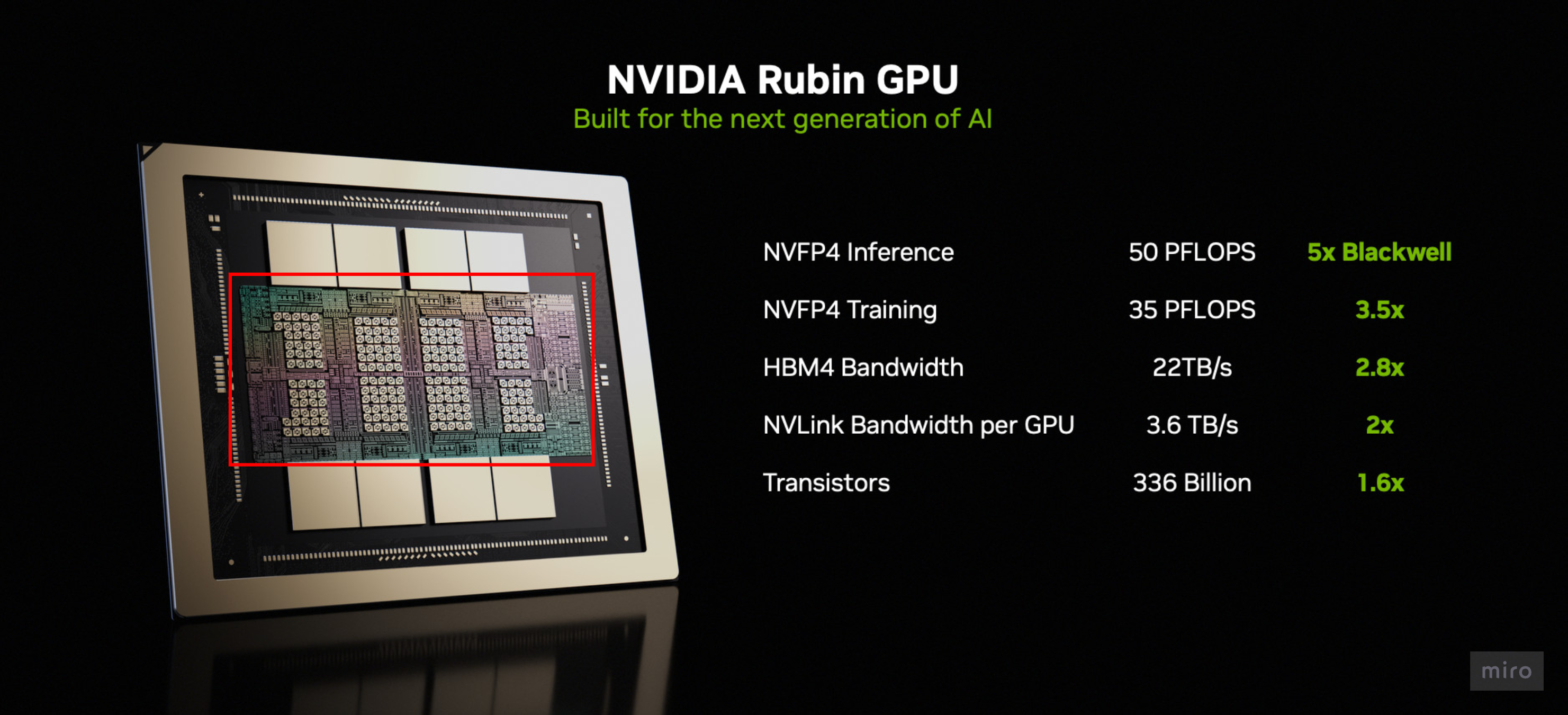
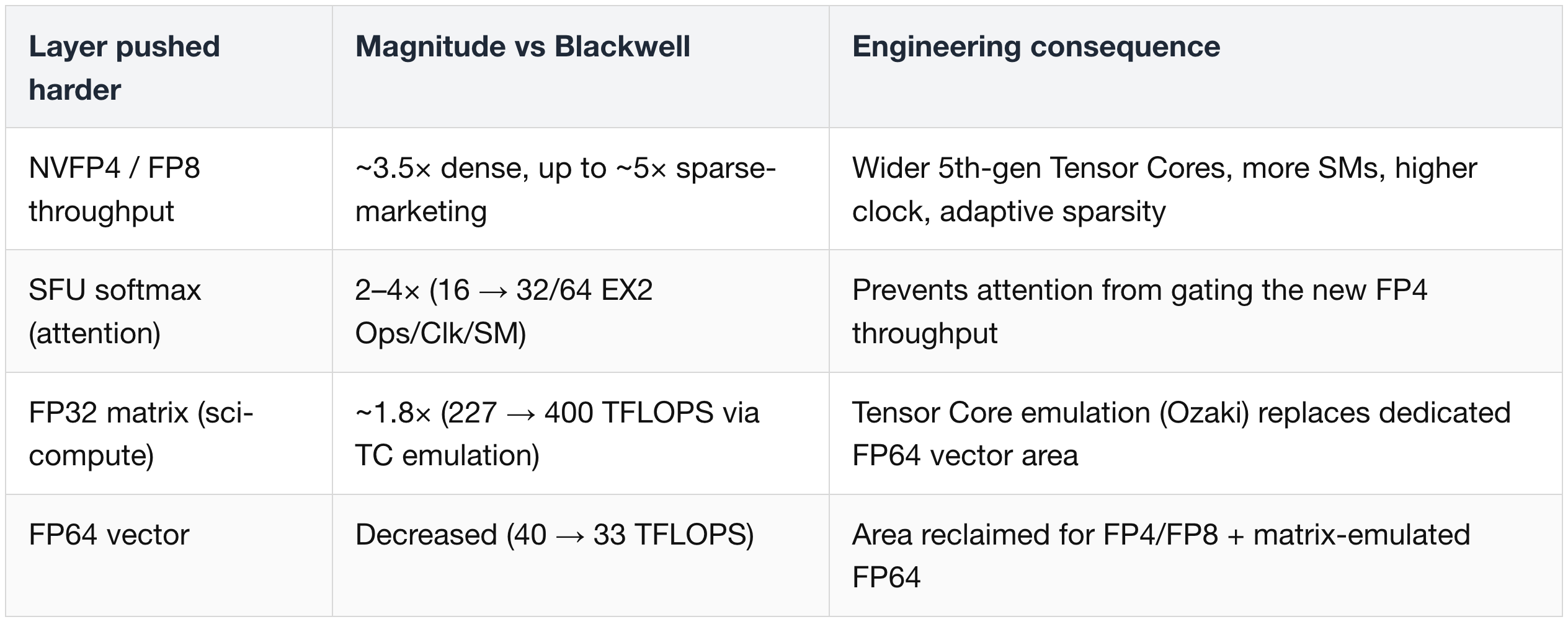
The 35 PFLOPS dense FP4 figure (3.5× over GB200) is achieved by three compounding levers:
- SM (Streaming Multiprocessor) count: 160 → 224. An SM is the basic building block of an Nvidia GPU — a small processor containing CUDA cores (general-purpose math units), Tensor Cores (matrix-math units), registers, and shared memory. A modern GPU is essentially hundreds of SMs running in parallel.
- 5th-gen Tensor Cores with width doubled to 32,768 FP4 MACs per SM per clock. A MAC is a multiply-accumulate operation (a × b + c) — the core operation of matrix multiplication, which dominates neural network math.
- Clock: 1.90 GHz → 2.38 GHz (+25%). The GPU's internal cycle rate; faster clock means more operations per second per unit of silicon.
The sections below move outward from the SM, through memory, I/O, precision/sparsity, power, and finally the package — each one driven by the section before it.
(1) Process Node & Die Structure
Rubin moves to TSMC's 3nm process and disaggregates I/O into chiplets, while keeping Blackwell's two-die + 8-HBM-stack layout.
- "Disaggregation" means breaking the chip into multiple smaller pieces (chiplets) that are then connected on the same package, instead of building everything onto one giant monolithic die.
- "I/O" (input/output) refers to the parts of the chip responsible for talking to the outside world — primarily NVLink to other GPUs, and NVLink-C2C to the CPU.
The compute dies stay reticle-sized and spend their area on more SMs and wider Tensor Cores instead of I/O. The NVLink-C2C and NVLink 6 I/O blocks become separate chiplets that can be designed and yielded independently of the logic dies. ("Yielded" refers to manufacturing yield: when a chip is broken into smaller pieces, manufacturing defects only ruin small pieces instead of the whole monolithic die, so a larger fraction of total silicon is usable.)
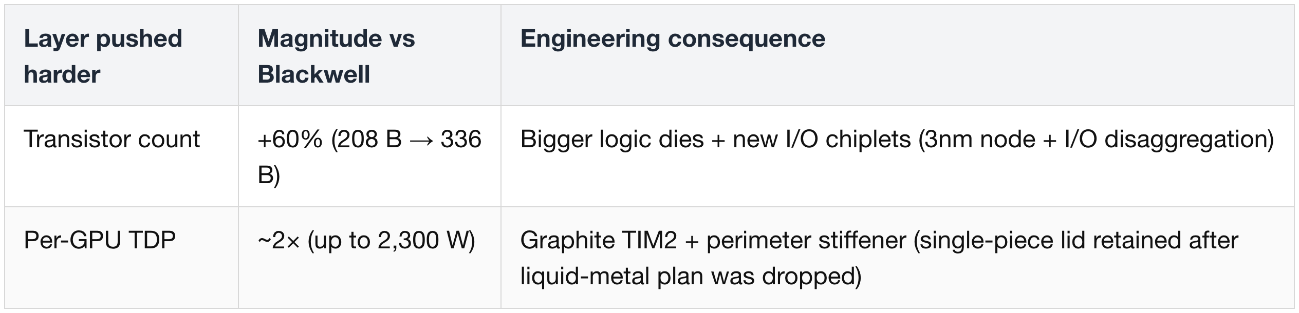
Transistor count rises +60% from 208 B (Blackwell) to 336 B (Rubin), driven by bigger logic dies, the new I/O chiplets, and the doubled Tensor Cores.
(2) Compute: SMs, 5th-Gen Tensor Cores, SFUs
The per-SM Tensor Core delta drives the FP4/FP8 scaling story. The width of a Tensor Core determines how many multiply-accumulate operations it can perform per clock cycle on each SM:
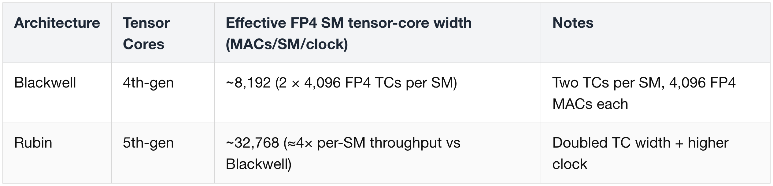
Notably, the Tensor Core width doubling only applies to NVFP4 and FP8.
- The wider formats — BF16 and TF32 — remain unchanged from Blackwell, resulting in FP16 performance scaling only 1.6× of Blackwell. BF16 (bfloat16) and TF32 (Nvidia's TensorFloat-32) are 16- and 19-bit formats traditionally used for AI training; they offer more numerical range than FP16 at the cost of being wider than FP8/FP4.
- This architectural decision reflects NVIDIA's belief that most training and inference workloads will move away from TF32 and BF16 and onto FP8 and FP4.
Special Function Units (SFUs). SFUs are the small math units inside each SM that handle "transcendental" operations — exponentials, logarithms, sines, reciprocals — which are far more complex than basic multiply/add.
- Rubin widens the SFU path. Softmax acceleration (measured in EX2 operations per clock per SM — EX2 means 2^x, the exponential operation that softmax depends on) rises from 16 (Blackwell) to 32 (FP32) / 64 (FP16) on Rubin, a 2–4× lift on the exp/softmax math that dominates the attention block of transformer models.
- (Softmax converts a vector of arbitrary numbers into a probability distribution, and the "attention" mechanism — which lets the model weigh which earlier tokens matter for predicting the next one — calls softmax billions of times per inference.)
- Without this SFU widening, attention kernels would bottleneck the new FP4 throughput.
Converged AI + scientific computing. Rubin rebalances FP32/FP64 throughput to favor AI-style matrix workloads. FP64 is the 64-bit double-precision format used by traditional scientific simulation codes (climate, fluid dynamics, computational physics). "Vector" operations are element-wise math on arrays; "matrix" operations are large matrix-matrix multiplications, which Tensor Cores accelerate.
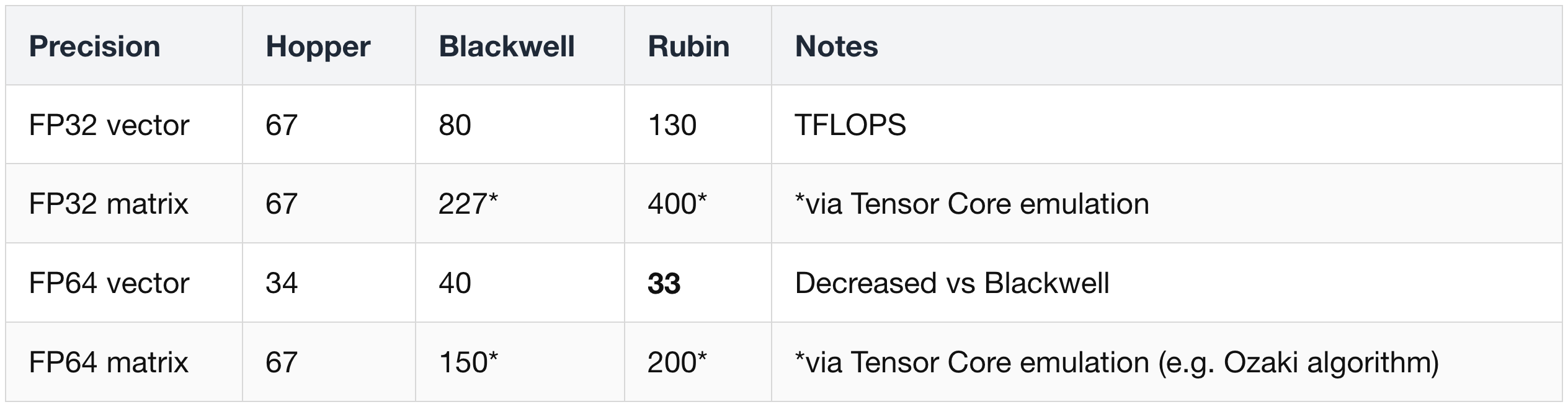
FP64 vector throughput drops slightly from Blackwell, because Nvidia is reclaiming that silicon area for FP4/FP8 and Tensor Cores.
- Scientific codes that need FP64-class accuracy on matrix work are expected to route through "Tensor Core matrix emulation": the FP64 result is produced by running multiple lower-precision Tensor Core passes and stitching the results together with carefully chosen error-correction terms.
- The Ozaki algorithm is one such technique that delivers FP64-equivalent accuracy on low-precision hardware, and Nvidia's cuBLAS library (its standard linear-algebra kernel library) ships with this emulation. FP64 vector still matters for codes whose performance is gated by memory bandwidth rather than compute throughput.
(3) Memory Subsystem — HBM4
Rubin moves from HBM3E (the generation used in Blackwell) to HBM4:
- Bus width per stack doubled vs HBM3E. "Bus width" is the number of parallel wires connecting the HBM stack to the GPU — more wires means more data per clock.
- Pin speed: 10.8 GT/s (gigatransfers per second — how fast each wire toggles).
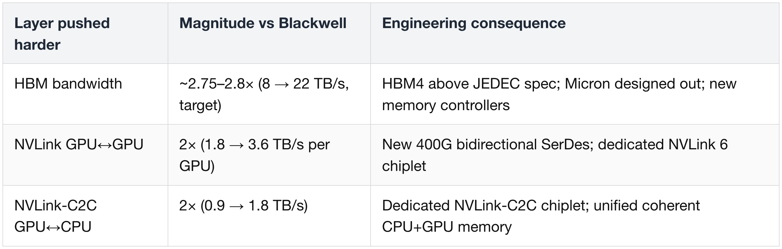
- Total bandwidth target: 22 TB/s, ≈2.75–2.8× Blackwell's 8 TB/s, at the same 288 GB capacity as GB300.
- Originally announced at GTC 2025 as 13 TB/s; Nvidia raised the target afterward.
- Paired with new memory controllers (the on-die logic that orchestrates reads and writes to HBM) and tighter compute-memory integration to keep the SM pipelines fed under load.

Why the bandwidth upgrade was forced. Under the original 13 TB/s spec, AMD's MI450 would have shipped with higher memory bandwidth than Rubin.
- To stay ahead, Nvidia demanded HBM4 pin speeds above what JEDEC standardized. JEDEC (Joint Electron Device Engineering Council) is the industry body that sets official memory specifications — every DRAM supplier designs against the JEDEC standard.
- Nvidia is effectively asking SK Hynix, Samsung, and Micron to overclock past the official spec, which puts the burden on the memory suppliers to validate parts at speeds the spec does not guarantee.
HBM4 Supplier Pin-Speed Dynamics
The three-way HBM race has a clear ordering at the Rubin generation:
- SK Hynix — currently leading on HBM4 pin-speed qualification. Expected to ship the first Rubin-grade HBM4 at the target 10.8 GT/s.
- Samsung — close behind SK Hynix; in qualification at Nvidia. Expected to be a second-source supplier as Rubin volume ramps.
- Micron — significantly behind on HBM4 qualification, effectively designed out of Rubin HBM4. This is a meaningful commercial blow, because HBM is the single most expensive component in the GPU package after the logic die itself.
What this means in practice:
- Initial Rubin shipments will likely land closer to ~20 TB/s (not the 22 TB/s headline target), because suppliers can't yet sustain the full 10.8 GT/s pin speed at production volumes.
- Pin-speed qualification is the new bottleneck — when you ask suppliers to validate parts above the JEDEC specification, you also accept that yields and binning ratios become Nvidia-specific rather than industry-standard. That's a real risk on supply continuity.
- The "Micron designed out" outcome ripples through the AI hardware supply chain: Micron's HBM revenue exposure to Nvidia drops sharply in 2026, while SK Hynix and Samsung gain incremental share.
Until Rubin's pin-speed targets actually qualify, the headline 22 TB/s should be treated as an aspirational spec rather than a guaranteed shipping number.
(4) I/O Chiplets — NVLink-C2C, NVLink 6, and Coherent Memory
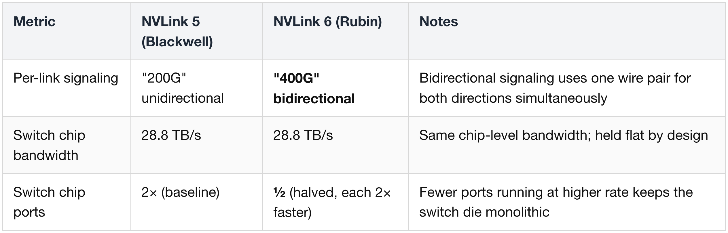
Off-die communication on Rubin is split across two dedicated I/O chiplets, both new in this generation. NVLink is Nvidia's proprietary high-bandwidth chip-to-chip interconnect — much faster than standard PCIe (the industry interface used to connect GPUs to motherboards). The absolute numbers:

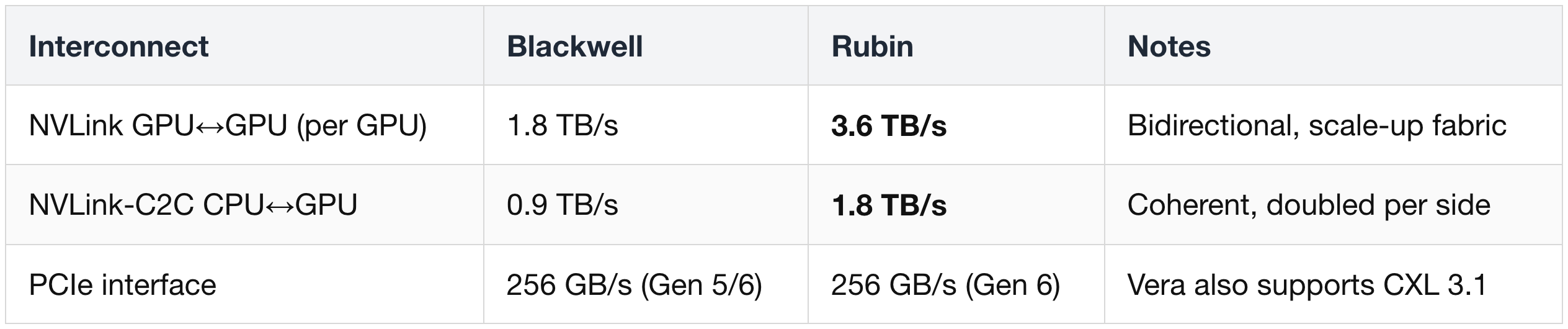
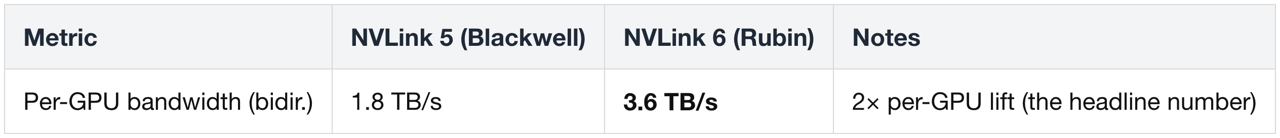
1) NVLink 6 chiplet (GPU ↔ GPU, rack-scale)
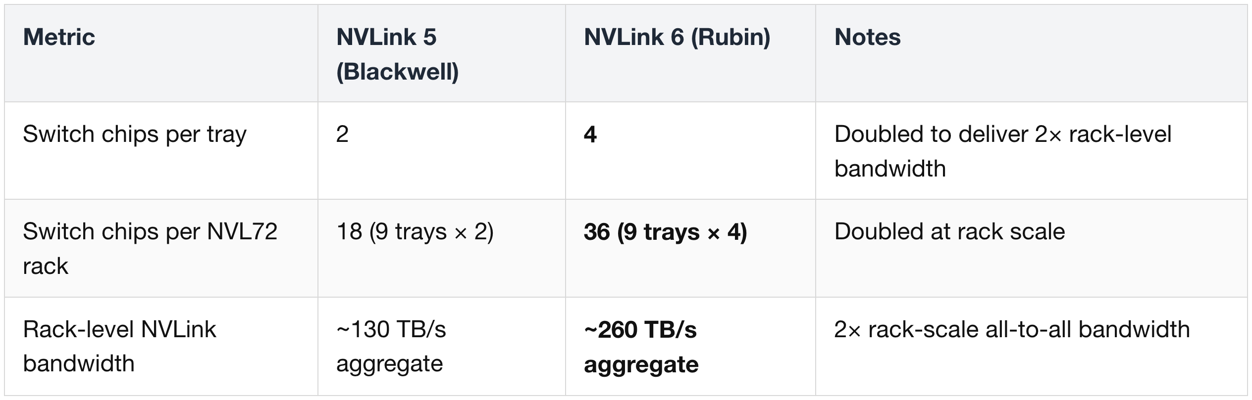
The chiplet provides 36 custom "400G" SerDes links, delivering 2× NVLink bandwidth (3.6 TB/s per GPU) to all 71 other Rubin GPUs in the NVL72 rack.
- SerDes stands for "Serializer/Deserializer" — these are the circuits that convert the GPU's wide parallel data into a fast serial stream over a single wire (or wire pair) and back again.
- The "400G" is in quotes because it is achieved through bidirectional signaling: a single wire pair runs at 200G per direction simultaneously, summing to 400G of total traffic.
- This same trick lets the NVLink 6 Switch keep a single monolithic 28.8 TB/s switch die with half the ports of NVLink 5 (Blackwell-era) running at double the rate.
- The 72-GPU topology is "full all-to-all", meaning any GPU can talk directly to any other GPU at full bandwidth without going through an intermediate hop.
NVLink 5 (Blackwell) vs NVLink 6 (Rubin) — key numerics. Context: same Oberon rack family (2024 → 2026), same full all-to-all topology across 72 GPUs. The deltas split into four layers — what each GPU sees, what the switch silicon does, how the rack aggregates it, and what extra in-switch capability comes with it.
What each GPU sees
Switch silicon (per chip)
Rack aggregation
In-network compute (SHARP)
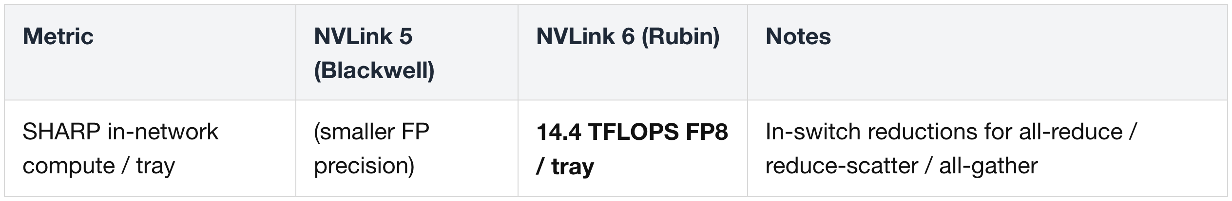
SHARP (Scalable Hierarchical Aggregation and Reduction Protocol)
- Nvidia's in-network compute feature: instead of every GPU sending its data to a central GPU for aggregation, the NVLink switch itself performs reduction math (e.g., summing values from all 72 GPUs) directly in the switch silicon as data flows through.
- This is critical for training, where models constantly need to compute "all-reduce" (every GPU contributes a value, every GPU receives the sum), "reduce-scatter" (sum and split the result), and "all-gather" (collect everyone's data) operations.
- NVLink 6 switches provide 14.4 TFLOPS of FP8 in-network compute per switch tray.
This is also why the rack-level NVLink switch count doubles to 36 (4 chips per switch tray) without requiring a multi-die switch — the per-link rate is doing more of the work.
2) NVLink-C2C chiplet (GPU ↔ Vera CPU)
- "C2C" stands for chip-to-chip — this is the dedicated short-distance link connecting each Rubin GPU to its paired Vera CPU on the same module.
- Bandwidth is doubled to 1.8 TB/s, and the link is "coherent". A coherent interconnect means the CPU and GPU automatically share the same view of memory — when one updates a value, the other sees the new value without manual synchronization. This makes a unified address space possible that spans Rubin's 288 GB of HBM4 and Vera's 1.5 TB of LPDDR5X (a power-efficient DRAM type used as system memory).
Applications can treat both pools as a single memory space, which enables:
KV-cache offload from HBM to LPDDR5X.
- When a large language model is generating text, it must remember intermediate attention computations for every prior token — this is the "KV cache" (key-value cache).
- On long contexts (millions of tokens), the KV cache outgrows GPU HBM.
- Coherent CPU memory lets the GPU page parts of the KV cache out to the CPU's larger LPDDR5X without manual copying, extending effective context length.
Multi-model execution
- Multiple models held in CPU memory, paged into GPU HBM as needed.
Reduced data movement overhead for agentic workflows
(5) Sparsity & the 3rd-Gen Transformer Engine
- Rubin replaces structured sparsity with adaptive compression in the 3rd-gen Transformer Engine, changing how the marketing FLOPS figures should be read.
- "Sparsity" refers to exploiting zeros in the model's weights or activations: a neural network does massive amounts of matrix multiplication, and if half the numbers being multiplied are zero, those multiplications can be skipped. The hardware question is how you exploit those zeros without losing model accuracy.
Background — 2:4 structured sparsity (H100 / B200 era)
The earlier approach required, in every group of 4 numbers, exactly 2 to be zero.
- This rigid structure was simple for the hardware (the multiplier unit could pre-skip exactly half its work), but hurt model accuracy because it forced non-zero values to zero — the model had to lose information to fit the hardware's pattern. Programmers ignored it.
The industry started designing around its uselessness:
- GB300 (Blackwell Ultra) kept sparse FP4 flat and added 50% more dense FP4 instead,
- AMD's MI355X dropped sparsity support from its MXFP8/MXFP6/MXFP4 formats entirely to reclaim die area. (MX-prefixed formats are AMD's variants of micro-scaled low-precision number formats, conceptually similar to NVFP4.)
Rubin's approach — adaptive compression in the 3rd-gen Transformer Engine.
Instead of forcing the model into a fixed sparsity pattern, Rubin's Transformer Engine detects zeros dynamically and in-flight as data streams through the GPU.
- It eliminates the multiplications for whichever values actually happen to be zero, without forcing any non-zero value to become zero.
- It works automatically on existing Blackwell-trained models with no recompilation or new programming model.
Models tuned via PTQ or QAT get larger speedups, but the tuning is not required:
- PTQ (Post Training Quantization) — converting a model's weights from high precision (e.g., FP16) to a lower-precision format like FP4 after training is complete.
- QAT (Quantization Aware Training) — training the model with the quantization step simulated, so the model's weights settle into values that are more robust to being expressed in low precision.
The two FLOPS numbers:
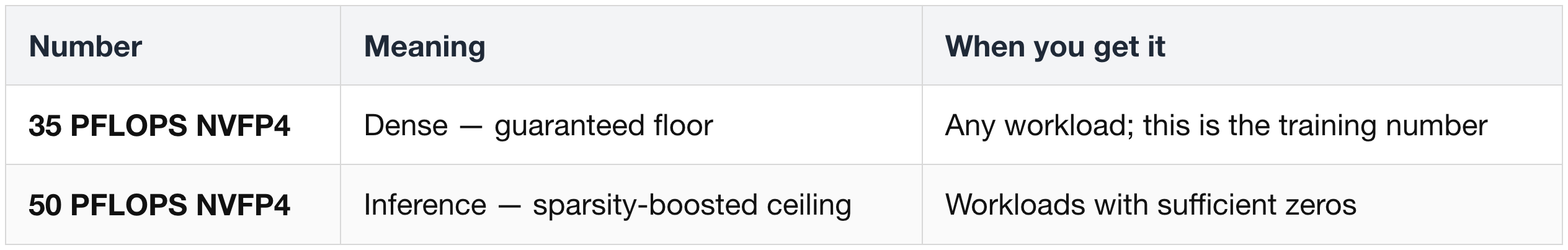
The marketing "5× over GB200" claim compares 50 PFLOPS (Rubin, sparsity-boosted) against 10 PFLOPS (GB200 dense FP4). The number is real but requires (a) the workload to be naturally sparse and (b) adaptive compression to deliver in practice. ML systems engineers — burned by 2:4 sparsity before — remain skeptical that 50 PFLOPS is anything more than a marketing peak.
(6) Power — Max-P vs Max-Q
- Per-GPU TDP rises from Blackwell's 1,000–1,400 W to 2,300 W, roughly 2×.
- TDP stands for Thermal Design Power: the maximum sustained power draw the chip is designed to operate at, which the cooling system must be sized to remove as heat.
- For reference, a high-end gaming GPU is ~450 W, and a residential microwave oven is ~1,000 W — Rubin draws more than two microwaves' worth of power per chip, all of which must be removed as heat by liquid cooling.
Supply chain rumors of "two SKUs" at 2,300 W and 1,800 W were a misreading. There is one chip, with two factory power profiles:
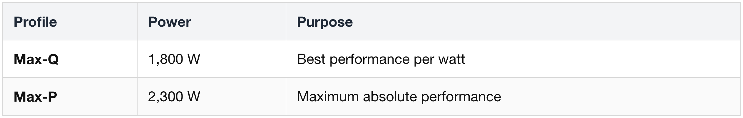
- Running Max-P uses 20% more rack power but delivers less than 20% more performance — diminishing returns at the top of the voltage/frequency curve. (At the top of any silicon's operating range, you must increase voltage rapidly to gain small frequency increases, and dynamic power scales with voltage squared.)
- Users can set any cap up to 2,300 W. Several hyperscalers historically run below the cap to optimize performance-per-watt and to fit within datacenter power budgets, which are increasingly the binding constraint rather than chip supply.
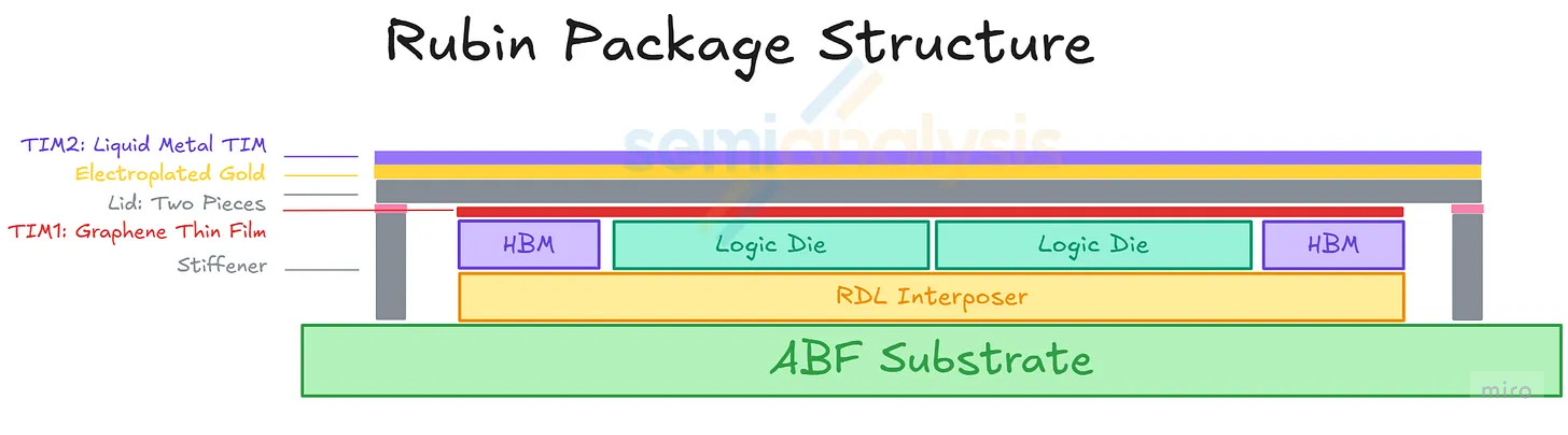
(7) Package, Mechanics, and Thermals
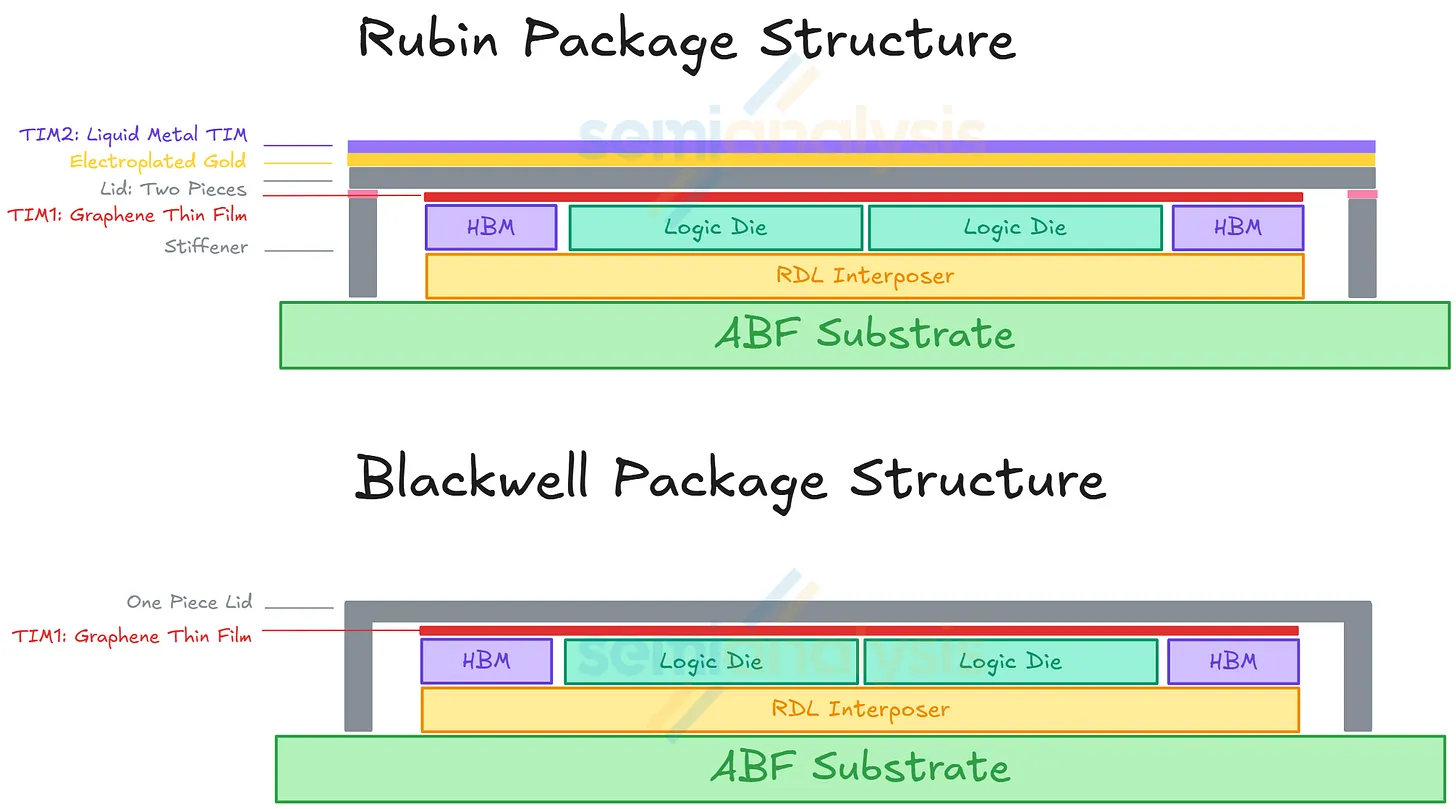
The silicon decisions above force the package — the assembly of materials surrounding and supporting the bare silicon dies — to be re-engineered. The bottom half of the package is unchanged from Blackwell.
Reading bottom to top:
- ABF substrate — the package's "motherboard," a multilayer organic board (made of Ajinomoto Build-up Film, the layer material) that fans out the dies' microscopic connections to large solder balls that connect to the rest of the system.
- RDL interposer — a re-distribution layer that sits between the dies and the substrate, with microscopic copper traces routing the thousands of connections from each die out to the substrate below.
- Two logic dies + 8 HBM stacks — the actual compute silicon and its memory stacks.
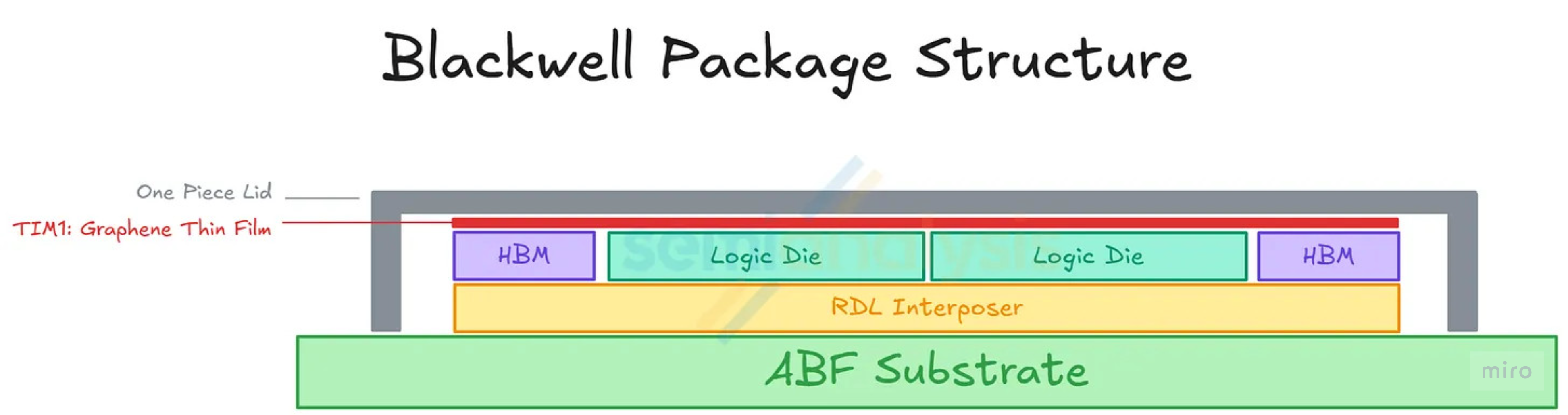
The top half is where Rubin diverges.
- The "lid" (also called the integrated heat spreader, or IHS) is the flat metal cover that sits over the dies;
- it spreads heat out evenly and provides mechanical support against bending.
Blackwell stack
- TIM1 (graphene thin film) on the dies. TIM stands for Thermal Interface Material — the substance between two metal/silicon surfaces that fills microscopic gaps and conducts heat across them.
- Single-piece lid covering both dies.
- Cold plate (the liquid-cooled metal block) sits directly on the lid.
Rubin: Original plan vs Final design
Rubin's package was originally announced with four new elements stacked above the dies — but during qualification (early May 2026), Nvidia backed off two of them. The reference architecture and the production architecture are now different in two places:
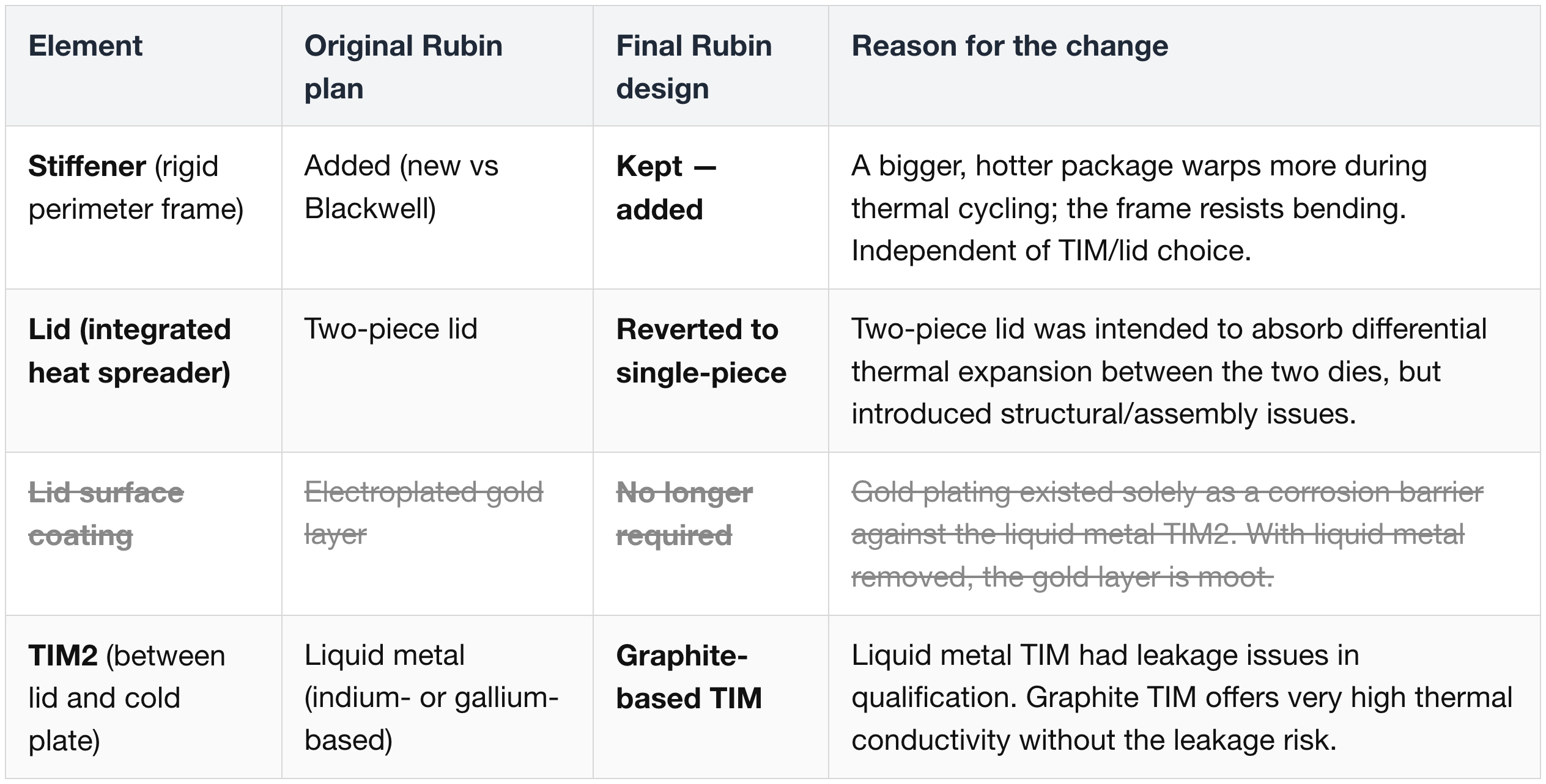
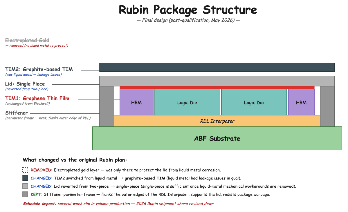
Why the changes happened.
- Rubin's chip-level TDP rose to 1,800–2,300 W.
- The traditional thermal paste used on Blackwell cannot move that much heat reliably, so a new TIM2 was needed.
- Nvidia's first choice was liquid metal (indium- or gallium-based alloys that stay liquid at operating temperature, filling microscopic gaps and conducting heat 5–10× better than paste).
- But liquid metal is mechanically fragile — it can creep, wick along surfaces, and corrode copper into brittle intermetallic compounds. During qualification, Nvidia hit leakage issues that the gold-coated lid + two-piece lid scheme was unable to contain reliably.
Nvidia's response was to switch the final TIM2 to a graphite-based thermal interface and revert the lid to a single-piece design.
- Graphite TIMs (typically thin pyrolytic graphite or graphite-composite sheets) are mechanically stable, do not flow or wick, and do not corrode metal
- they conduct heat well enough to handle Rubin's 2,300 W without the engineering risk of liquid metal.
- With graphite TIM2 in place, the gold corrosion barrier and the two-piece-lid mechanical workaround become unnecessary.
Schedule impact. This series of late-stage thermal architecture changes — resolving liquid-metal leakage, switching TIM material, and reorganizing the lid — pushed Rubin's volume production and shipment timeline back by several weeks. As a result, Rubin's shipment share for 2026 has been lowered.
The chain of consequences (final design).
- Rubin runs at 2,300 W → the traditional Blackwell thermal paste between lid and cold plate cannot move heat fast enough → a higher-conductivity TIM2 is required.
- Liquid metal TIM (the first choice) had leakage and copper-corrosion problems that the gold-coating + two-piece-lid scheme could not fully contain → Nvidia switched to a graphite TIM2.
- With graphite TIM2, the gold corrosion barrier is no longer required, and the package can revert to a single-piece lid — both materials are thermally and mechanically compatible with the simpler design.
- The stiffener stays — the bigger, hotter package still warps without it, regardless of which TIM is used.
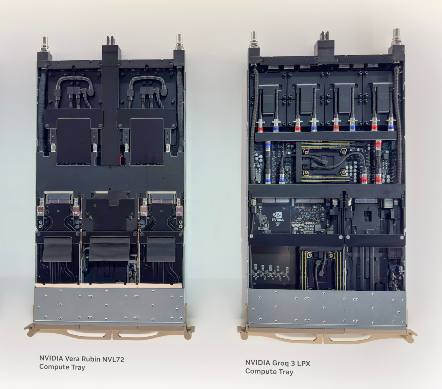
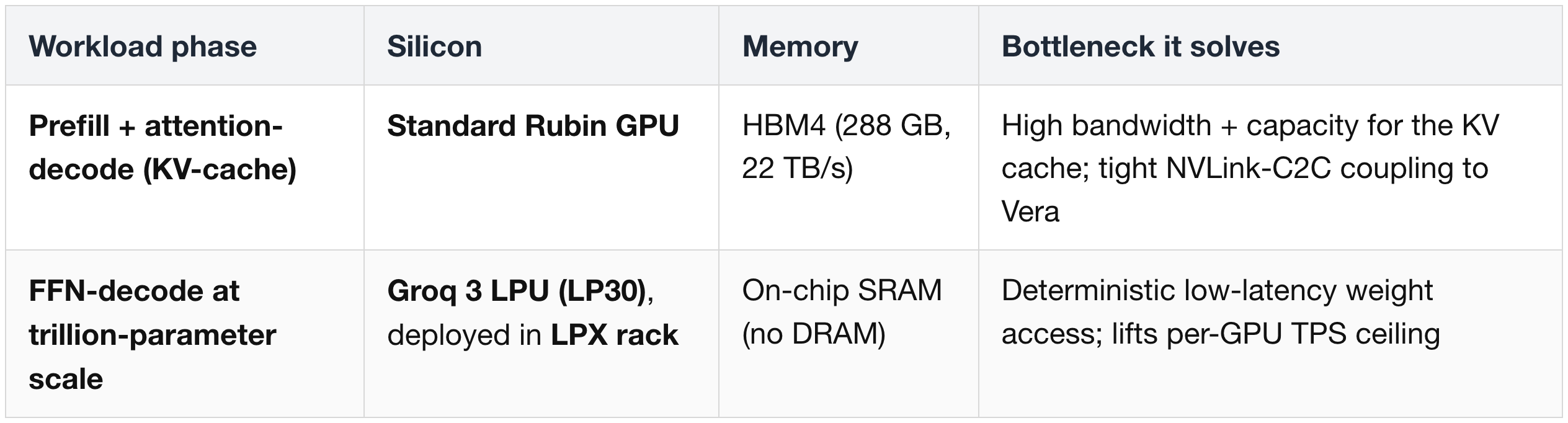
(8) Workload-Specialized Silicon — Groq 3 LPU (the Seventh Chip)
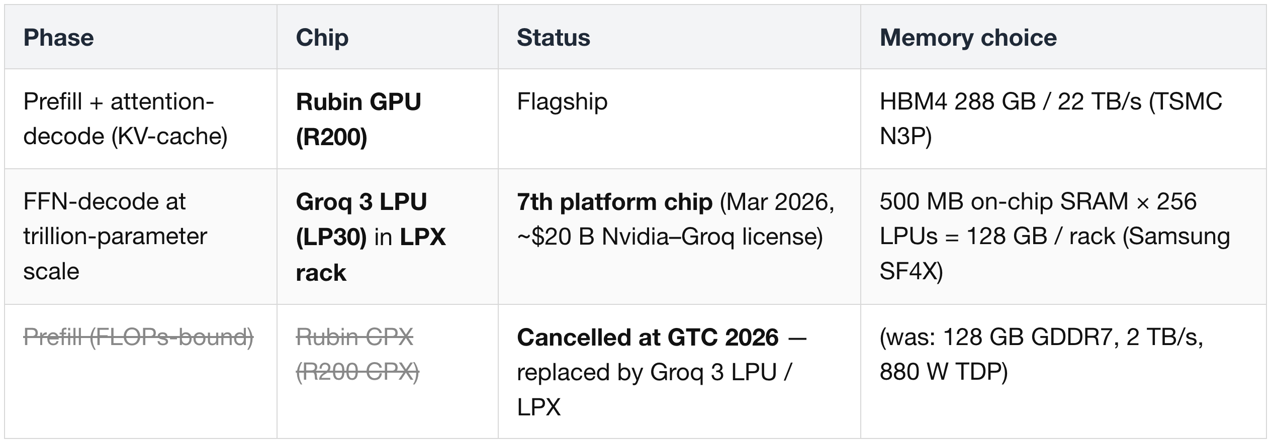
Rubin isn't just one chip. The platform now ships with the Groq 3 LPU (chip; codename LP30) deployed inside the Groq 3 LPX rack alongside the flagship Rubin GPU — a separate compute architecture that takes over the entire inference-specialization workload Nvidia originally planned to address with the now-cancelled Rubin CPX.
Naming convention: LPU is the individual chip (Groq 3 LPU = LP30); LPX is the unified rack system (256 LPUs across 32 trays). The two are not interchangeable.
This is the same architectural shift Nvidia has been pointing at since the AI Infra Summit Sep 2025 — moving from "one universal GPU" to workload-specialized silicon at the rack level, formalizing the prefill / decode disaggregation production inference frameworks have been demanding — just executed via license rather than in-house silicon.
Historical Note — Rubin CPX (Cancelled at GTC 2026)
Before the Groq deal, Nvidia had its own purpose-built inference accelerator on the roadmap: Rubin CPX (R200 CPX). The cancellation matters because the CPX design intent and tradeoffs explain why the Groq 3 LPU exists in the platform at all.
What CPX was supposed to be
- 128 GB GDDR7 memory, ~2 TB/s bandwidth, 880 W TDP, PCIe Gen 6 scale-up (no NVLink) — vs standard Rubin's 288 GB HBM4 at 22 TB/s and 2,300 W.
- 30 PFLOPS NVFP4 dense compute (2× B300's 15 PFLOPS) — optimized for FLOPs-heavy prefill workloads where HBM bandwidth is structurally underutilized.
- TSMC N3P (same node as standard Rubin), but a separate-tapeout die with a fundamentally different memory PHY (GDDR7 vs HBM4) — not a downscaled / die-harvest variant.
- Three deployment options had been on the table: standard NVL72 (no CPX), CPX-integrated trays, and CPX-dual-rack. The dual-rack path was the leading direction prior to cancellation.
Why it was cancelled
- Removed from Nvidia's roadmap at GTC 2026 (Mar 2026) — announced at AI Infra Summit Sep 2025, never reached production tapeout.
- Replaced by the Groq 3 LPX Rack, a fundamentally different SRAM-based decode-acceleration architecture acquired via Nvidia's ~$20 B Groq license deal.
- Jensen Huang clarified on the Q1 FY2027 earnings call (May 2026) that what analysts had been calling "Rubin CPX" is now "LPX," scoping the use case to "low latency and high token rate" but "low throughput, low model size capacity, and limited context processing" — i.e., a niche product, not a broad replacement for standard Rubin.
The CPX → Groq 3 LPU silicon swap is the headline structural change of the Rubin platform: Nvidia chose to license external silicon rather than try to extend its own GPU into the niche inference acceleration role.
Groq 3 LPU + LPX Rack — The Replacement Inference Stack
- Groq 3 LPU (chip; codename LP30) — announced March 16, 2026 as the seventh chip in the Vera Rubin platform (~$20 B Nvidia–Groq licensing deal).
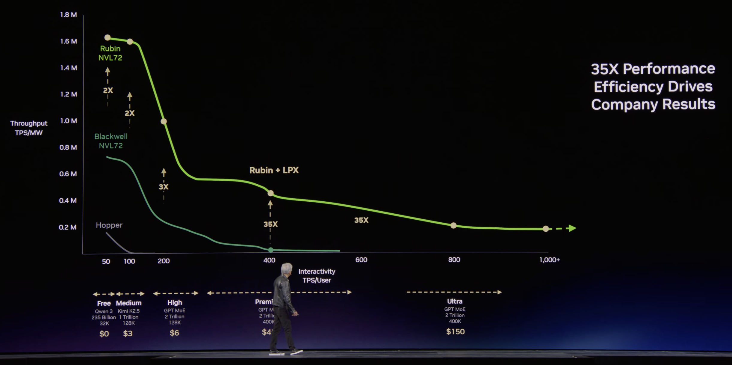
- Targets the decode phase — specifically the bandwidth-starved feed-forward network (FFN) matrix multiplications that dominate token-by-token generation at trillion-parameter scale, where Rubin's HBM-bound throughput hits a per-GPU TPS ceiling.
- Deployed as the Groq 3 LPX rack — a unified rack system housing 256 LPUs across 32 trays (8 LPUs / tray), with 128 GB aggregate SRAM and 40 PB/s aggregate bandwidth — designed to ship in Q3 2026 alongside Rubin.
The Groq 3 LPX Tray vs the Standard Rubin Compute Tray
Each tray inside the Groq 3 LPX rack is 1U liquid-cooled, with the same mechanical envelope as the standard Rubin NVL72 compute tray — drop-in compatible at the chassis level, but a completely different silicon population inside.
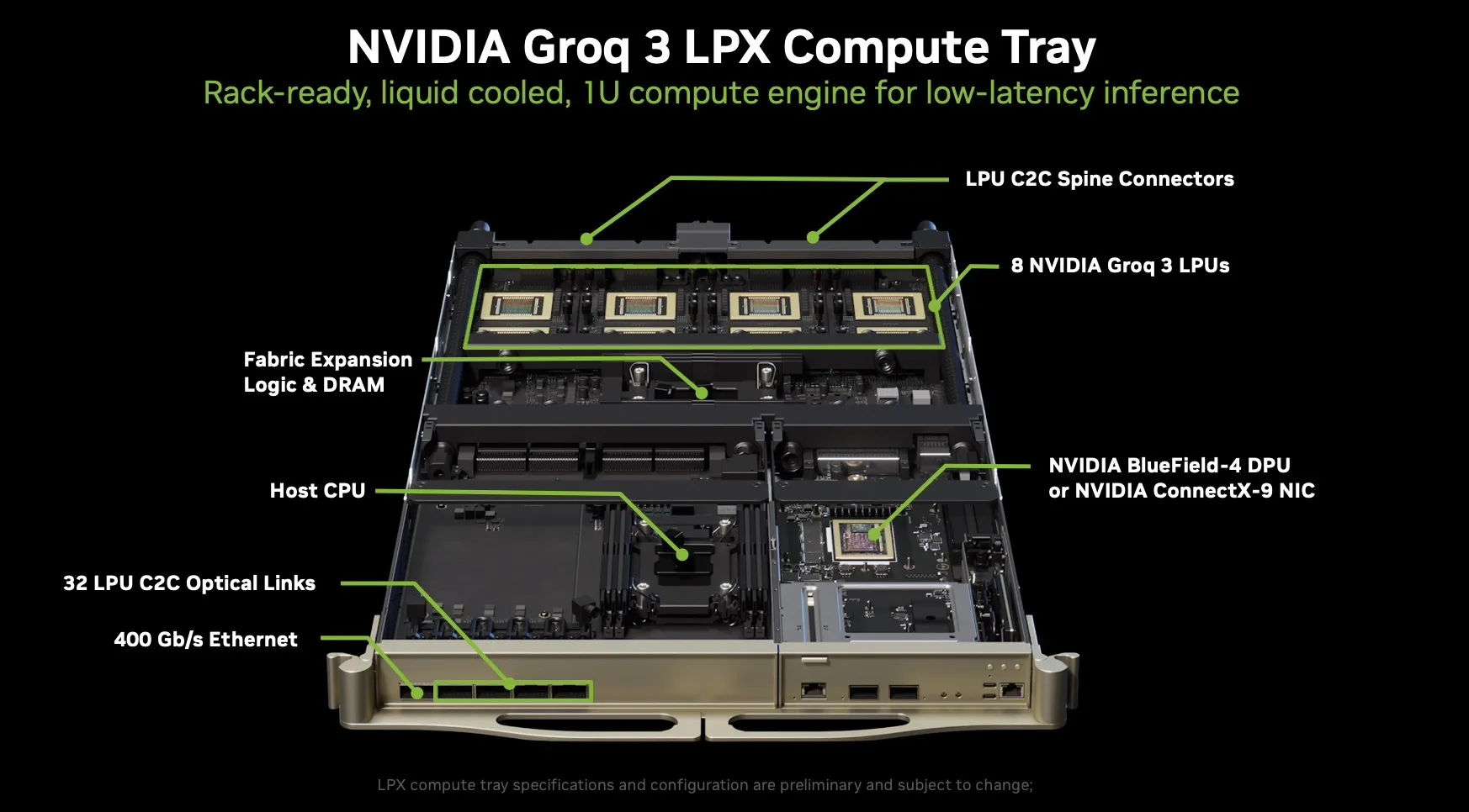
The annotated tray reveals the per-tray composition:
- 8× Groq 3 LPUs as the primary compute, with LPU C2C spine connectors carrying chip-to-chip traffic across the rack.
- Fabric Expansion Logic + DRAM module — provides extended scratch capacity for activations and the deterministic-fabric control plane (Groq's compiler-scheduled inter-chip routing).
- Host CPU at center handles orchestration and host-side I/O.
- NVIDIA BlueField-4 DPU or ConnectX-9 NIC on the front — same NIC/DPU SKUs as the Rubin tray, so the LPX tray plugs into the same scale-out fabric.
- 32× LPU C2C optical links for inter-tray expansion of the LPU domain.
- 400 Gb/s Ethernet front-panel for scale-out to the rest of the cluster.
The key takeaway: from the rack and fabric's point of view, an LPX tray looks like a Rubin tray (same NIC/DPU, same Ethernet, same chassis), which is what lets hyperscalers compose mixed Rubin + LPX racks without re-architecting the network.
Why Decode Needs Its Own Silicon
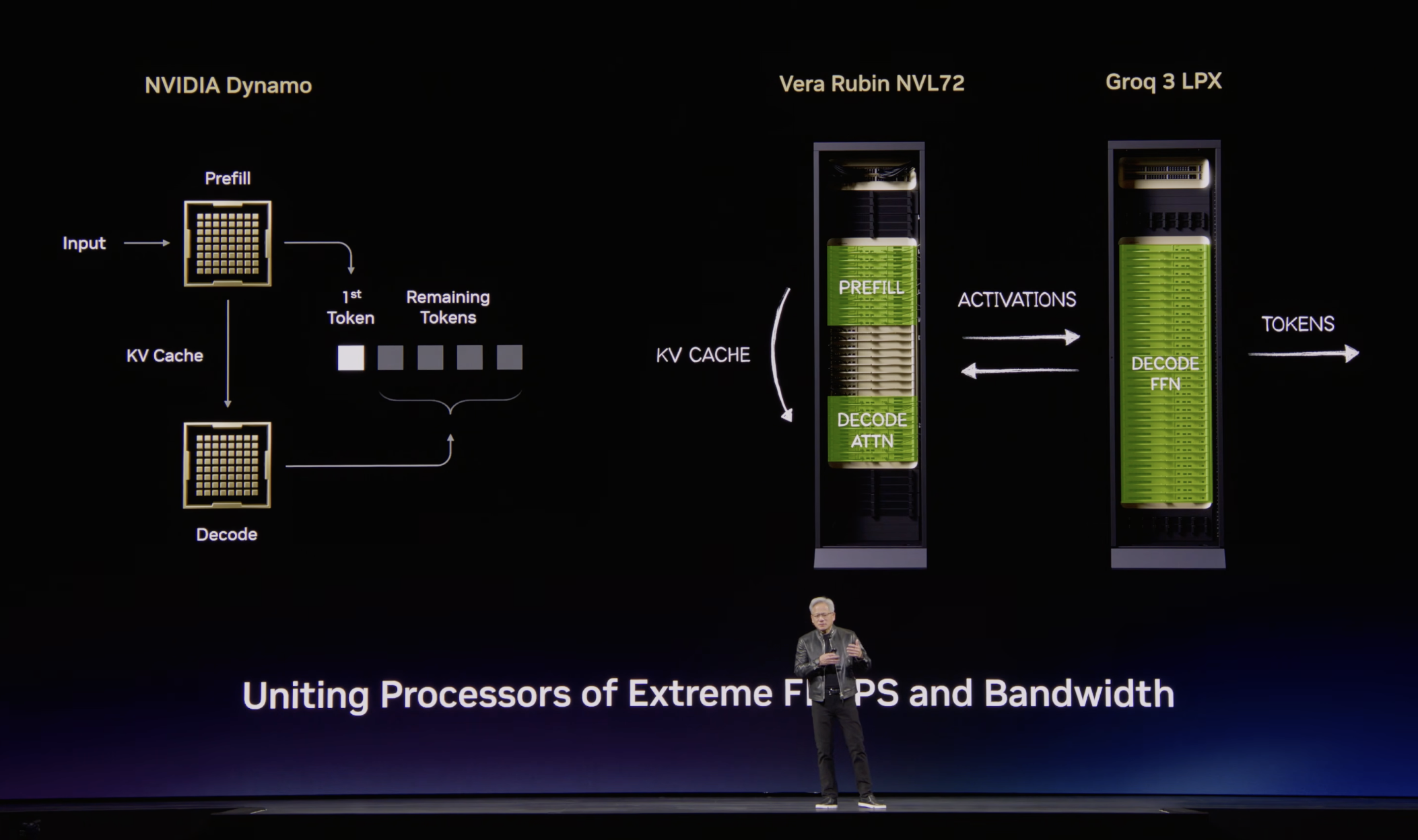
Decode throughput on conventional GPU silicon — including Rubin — degrades steeply as model parameter counts grow. The bottleneck is the weight-fetch pattern: every generated token requires the GPU to re-stream the model's weights through HBM, and HBM bandwidth (even at Rubin's 22 TB/s) cannot keep up once the model crosses the trillion-parameter range. The result is a per-GPU tokens-per-second ceiling that scales poorly:
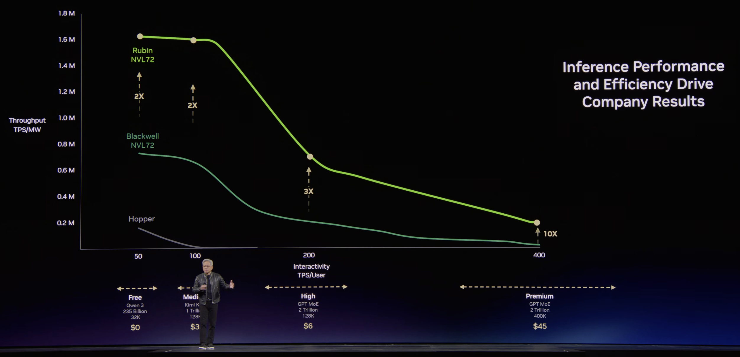
Layering Groq LPX into the decode path lifts this ceiling because Groq's architecture is built around a fundamentally different memory model:
How Groq's Architecture Differs (Overview, Not Deep-Dive)
Groq's chip family is built on the TSP (Tensor Streaming Processor) lineage — branded as LPU (Language Processing Unit) in its previous standalone form, and now LP30 as the Vera-Rubin-integrated variant inside the Groq 3 LPX rack. The architectural deltas vs. a GPU are:
- No HBM, no external DRAM. All weights and activations live in on-chip SRAM — 500 MB per LP30 chip (2.2× the 230 MB Gen-1 LPU baseline), delivering 150 TB/s per chip. Aggregate across the 256-LPU rack: 128 GB SRAM at 40 PB/s.
- Deterministic, statically scheduled execution. The compiler lays out every instruction's cycle-exact placement on the chip. No dynamic scheduling, no cache-miss latency, no memory-hierarchy variance — latency is predictable to the cycle, which is what low-latency token generation rewards.
- Optimized for the FFN matrix path. The systolic-style streaming compute fabric maps efficiently onto the dense GEMMs that dominate FFN execution during decode.
Foundry choice — Samsung, not TSMC. LP30 (Groq 3 LPU) is fabricated on Samsung Foundry's SF4X (4 nm) process, not TSMC 3 nm — making the LPU the platform's only non-TSMC primary silicon. Groq's roadmap stays on Samsung 4 nm for the LP35 refresh (2027), then moves to TSMC N3P with CoWoS-R packaging for the LP40 generation co-designed with Nvidia for the Feynman platform (2028).
Inter-chip fabric. Each LP30 has 96 C2C links at 112 Gb/s per lane, delivering 2.5 TB/s bidirectional per chip. Tray-level inter-rack scale-up runs over 32 optical lanes at the same 112 Gb/s, giving 3.6 Tb/s per tray and 14.3 TB/s aggregate per rack of inter-tray bandwidth — proprietary Groq SerDes, not industry-standard 200 G/400 G optics.
The trade-off Groq accepts: each chip has a small on-chip memory footprint, so large models must be sharded across many LP30 chips connected by Groq's deterministic inter-chip fabric. That cost is acceptable when the alternative is HBM-bound throughput on a GPU.
The Resulting Two-Tier Inference Stack
With Rubin CPX cancelled, Rubin platform inference splits across two silicon classes — Nvidia GPU + Groq LPU:
Why This Matters for the Architecture Story
- Rubin CPX was the first concrete example of Nvidia building workload-specialized in-house silicon — but it never reached production.
- The Groq 3 LPU (deployed in the LPX rack) is its replacement, via license rather than tapeout. When even the flagship GPU can't span all phases of inference economically, Nvidia chose to license external silicon and integrate it as a named platform chip rather than ship its own purpose-built variant.
- The architectural lesson is that the workload was real (and substantial — Nvidia walked through CPX, then a ~$20 B Groq deal to fill the gap), but the path to fill it was not an internal die. Expect more licensed-silicon integrations in future generations as workloads specialize further (Feynman's LP40 is already co-designed).
(9) Summary — How the Rubin GPU Story Hangs Together
Compute & Precision
Data Movement (Memory + Interconnect)
Silicon & Package
Rubin pushes NVFP4/FP8 throughput and HBM bandwidth aggressively, and every other change — chiplet disaggregation, NVLink generation, package mechanics, thermal stack — is the engineering consequence of those two choices.
Workload-Specialized Silicon Beyond the Flagship GPU
Vera Rubin is the first Nvidia platform where the AI factory is not built from one universal GPU.
Where to Read What — Series Map
| Part | Title | Scope |
|---|---|---|
| 1 | Platform Framing & Architecture Map | Blackwell → Rubin platform thesis, headline specs |
| 2 | Rubin GPU — Engineering Deep Dive (this part) | Process node, SMs, HBM4, NVLink-C2C, package, CPX + Groq 3 LPX |
| 3 | Vera CPU & the Networking Silicon Family | Vera CPU, NVLink 6 Switch, ConnectX-9, BlueField-4, Spectrum-6 |
| 4 | Rack Assembly — Trays, PCB, and Cooling | HGX vs NVL72, compute tray modules, cableless midplane, PCB upgrade, liquid cooling |
| 5 | Rack Power and the Networking Fabric | Power delivery, HVDC, tray↔rack wiring, scale-up NVLink 6, scale-out InfiniBand + Ethernet |
| 6 | Supply Chain — Master Reference | Suppliers by subsystem across the entire stack |