Vera Rubin Decoded Pt. 5 | Rack Power and the Networking Fabric
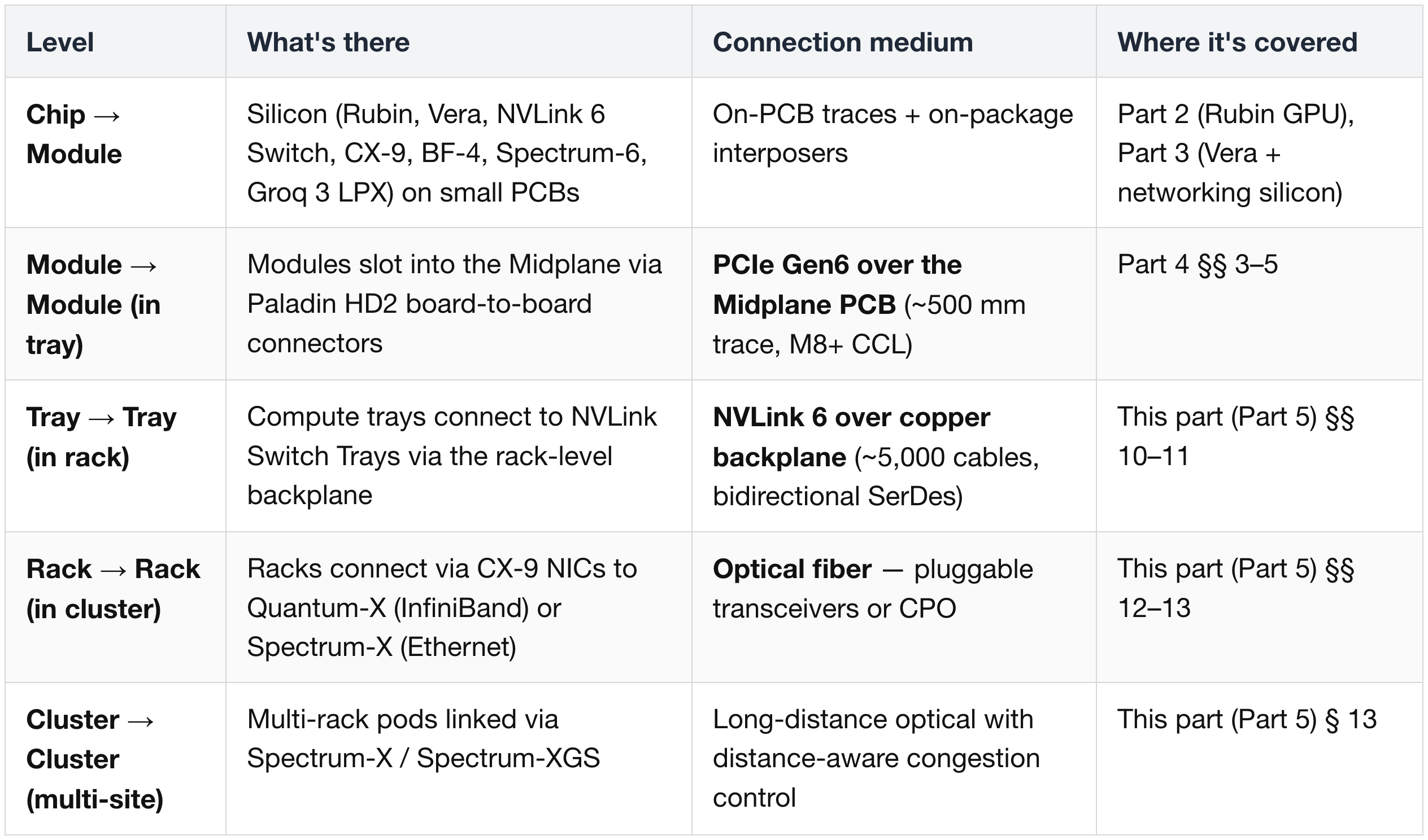
Where to Read What — Series Map
| Part | Title | Scope |
|---|---|---|
| 1 | Platform Framing & Architecture Map | Blackwell → Rubin platform thesis, headline specs |
| 2 | Rubin GPU — Engineering Deep Dive | Process node, SMs, HBM4, NVLink-C2C, package, CPX + Groq 3 LPX |
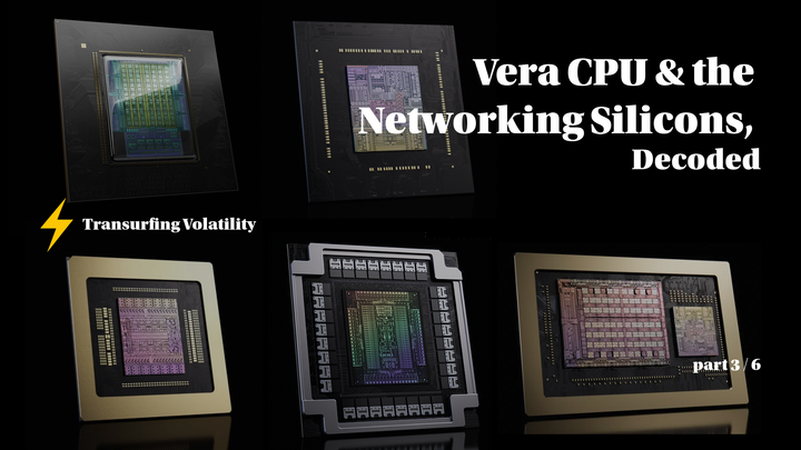
| 3 | Vera CPU & the Networking Silicon Family | Vera CPU, NVLink 6 Switch, ConnectX-9, BlueField-4, Spectrum-6 |
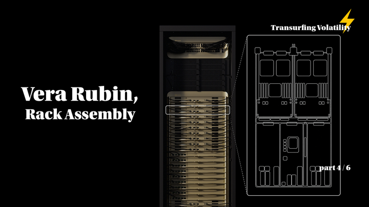
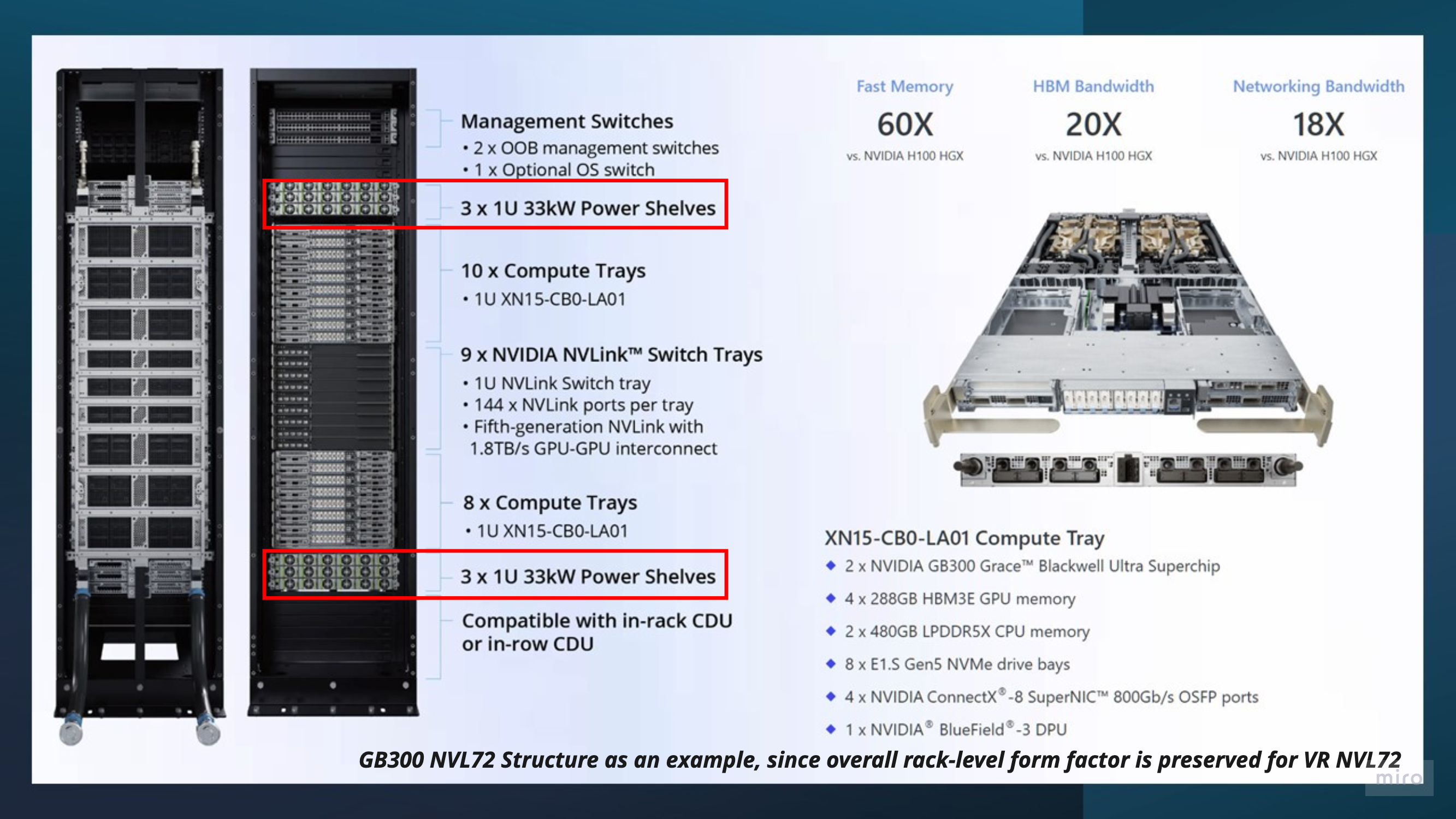
| 4 | Rack Assembly — Trays, PCB, and Cooling | HGX vs NVL72, compute tray modules, cableless midplane, PCB upgrade, liquid cooling |
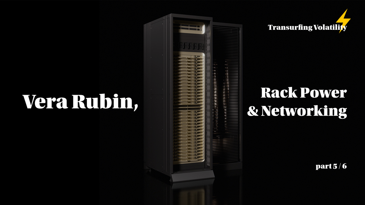
| 5 | Rack Power and the Networking Fabric (this part) | Power delivery, HVDC, tray↔rack wiring, scale-up NVLink 6, scale-out InfiniBand + Ethernet |
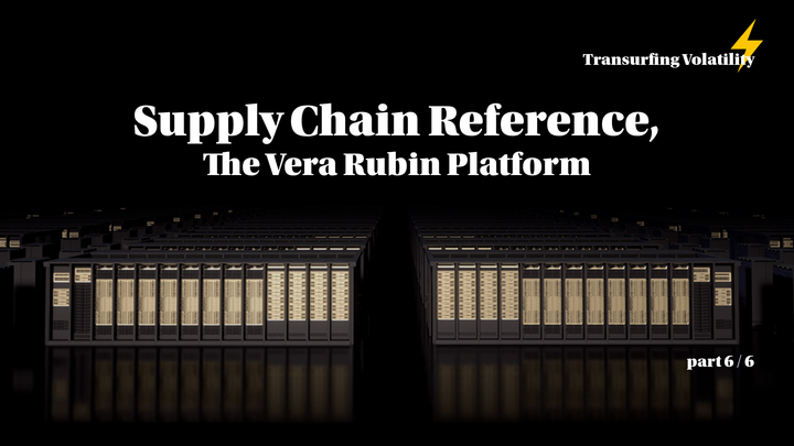
| 6 | Supply Chain — Master Reference | Suppliers by subsystem across the entire stack |
Continued from Vera Rubin Decoded — Part 4. Same NVL72 rack, now from power delivery outward through the networking fabric.
(8) Power Delivery — Chain from AC Mains to the Chip
Per-rack TDP: 180–220 kW (vs 120–140 kW for GB200/GB300). The power delivery chain has three steps:
Step 1: AC mains → 50 V DC (rack power shelves)
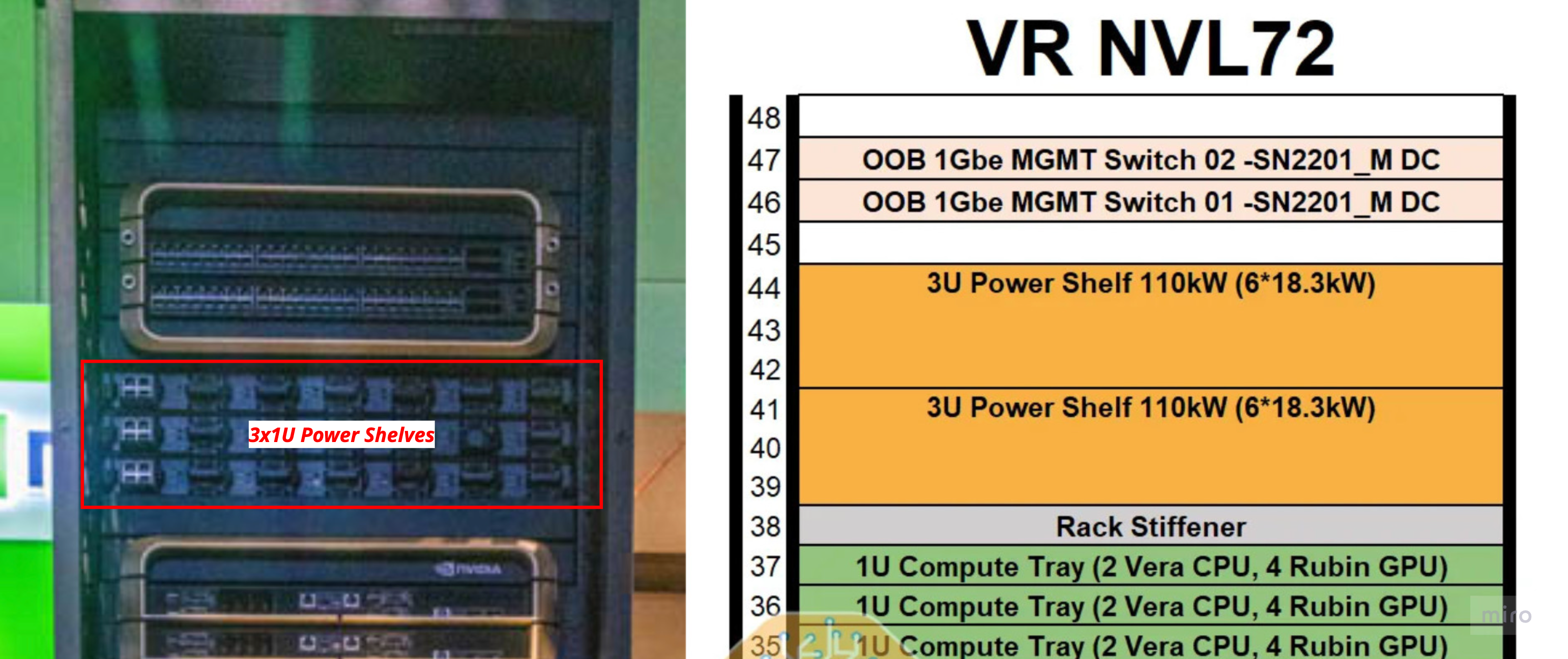
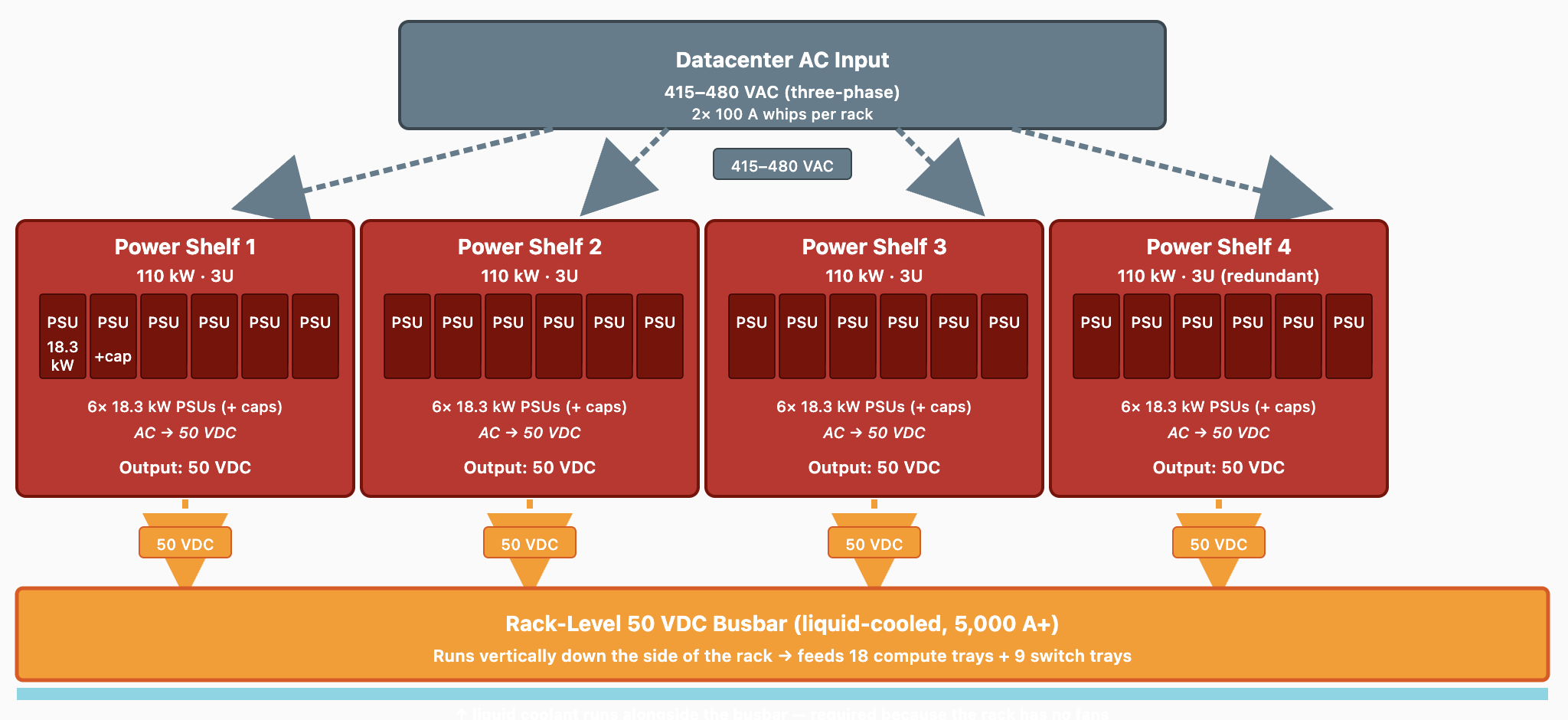
- 3-4× power shelves at the top and bottom of the rack, 110 kW each (N+1 redundancy → 330 kW deliverable for a 220 kW peak)
- Each shelf is 3U tall and contains 6× 18.3 kW PSUs with built-in capacitors
- Input: three-phase 415–480 VAC via two 100A whips
- Output: 50 VDC delivered to a liquid-cooled busbar rated at 5,000 A+ (vs 2,900 A for GB200)
- Why liquid-cooled? At this current level, the busbar itself dissipates significant heat, and the rack has no fans to remove it.
Step 2: 50 V busbar → compute tray (yellow dotted paths)
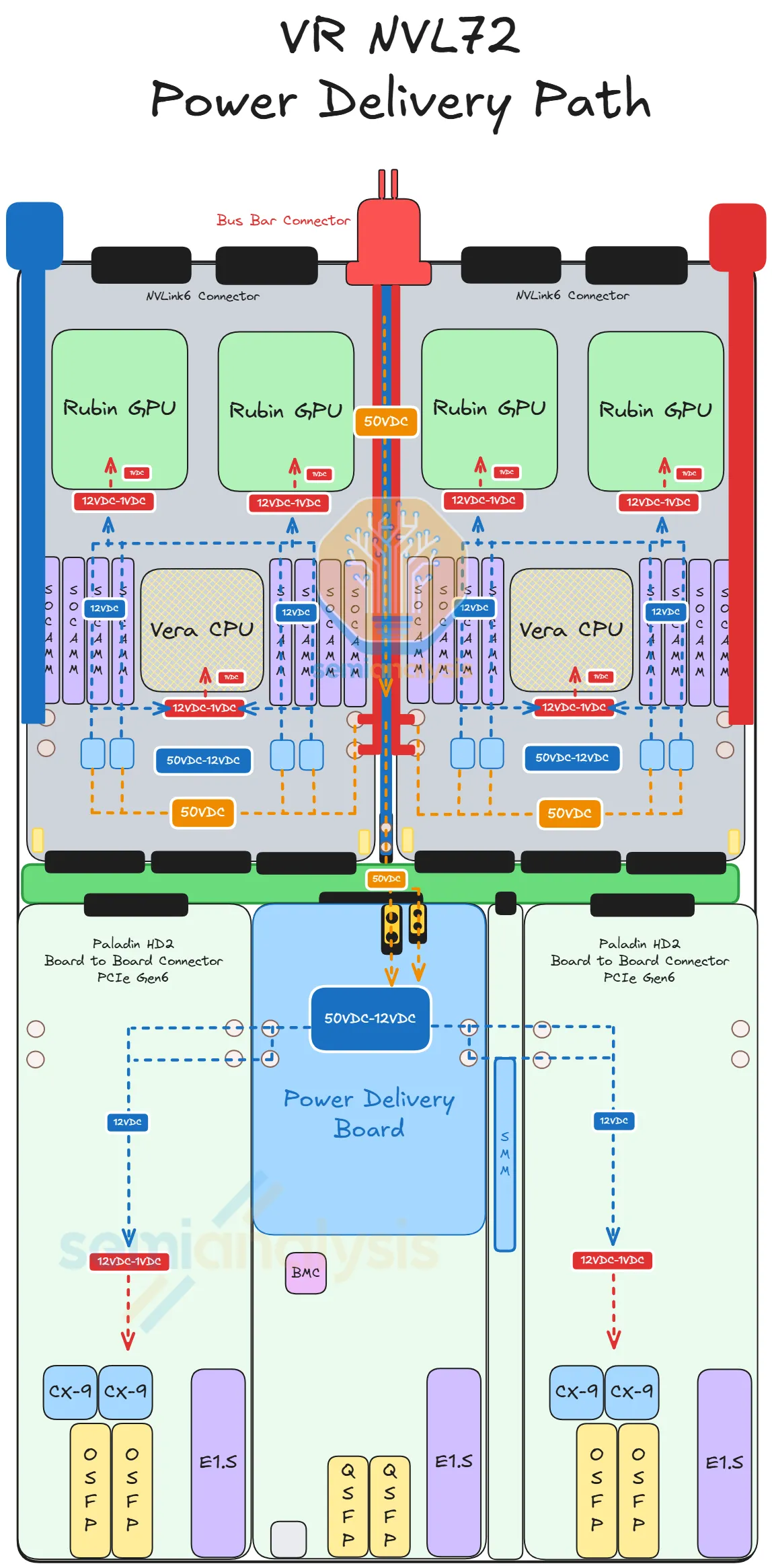
- Tray clips into the rack busbar at the back
- Internal busbar cables route 50 V to two destinations:
- Strata Modules (direct 50 V — they handle their own step-down because they draw too much current for a centralized 12 V rail to be efficient)
- Power Delivery Module at the front (which converts 50 V → 12 V centrally for the smaller modules)
Step 3: 50 V → 12 V → 1 V (on each board; blue dotted paths for 12V → 1V, red dotted paths for 12V → 1V)
- Strata board has its own IBC (Intermediate Bus Converter) for 50 V → 12 V, then VRMs for 12 V → ~1 V to feed the GPU/CPU dies
- PDB does the 50 V → 12 V conversion for the Orchid, BF-4, and Mgmt modules, then distributes 12 V to them via short busbars
Why 50 V instead of 12 V to the tray?
- Power loss in a wire scales with current squared (I²R), not voltage
- Delivering 4,800 W at 50 V = 96 A; at 12 V it would need 400 A
- That's 17× less power loss moving the higher-voltage form factor closer to the chip before stepping down
"Power sloshing" between Vera and Rubin
A feature carried over from GB300: the Strata board's 4,800 W power budget is shared dynamically between the 2 Rubin GPUs and 1 Vera CPU. Under GPU-heavy load, each Rubin can pull 2,300 W (leaving 200 W for Vera). When the GPUs idle or de-rate, Vera can pull more power. This avoids over-provisioning the power supply for worst-case-on-both-sides simultaneously.
(9) Rack-Level Power — HVDC, BBU/CBU, and Hyperscaler Variants
The reference design at rack level (4× 3U 110 kW power shelves → 50 V liquid-cooled busbar) was covered in § 8 Step 1. This section is about the variants hyperscalers deploy when they diverge from that reference — driven by per-rack TDPs now at 180–220 kW and trending toward 1 MW per rack in the next couple of generations.
Two main directions of divergence:
- Higher-voltage distribution — HVDC power racks feeding 50 V step-down shelves inside the GPU rack.
- Integrated energy storage — BBU + CBU shelves moved to an adjacent rack for peak shaving and grid bridging.
1) Option A — HVDC (High-Voltage DC) Power Racks
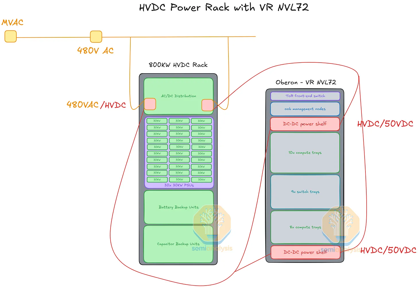
Some hyperscalers deploy a separate power rack running at much higher DC voltage and feed it horizontally to the GPU rack. Two voltage standards are in play:
- 800 VDC — Nvidia's specification
- ±400 VDC — OCP (Open Compute Project) specification
How HVDC delivery works
- AC mains → power rack converts to 800 VDC (or ±400 VDC) and distributes via thick conductors.
- Horizontal 800 VDC busbars (or cables) connect the power rack to adjacent GPU racks.
- Inside the GPU rack, DC-DC step-down shelves convert 800 VDC → 50 VDC, feeding the standard rack busbar.
- From there, the rest of the delivery path is identical to the AC reference design (see § 8).
Why HVDC matters
- Lower I²R losses on the long horizontal run between power and compute racks (the same I²R argument that justifies 50 V > 12 V inside the tray, just applied at a larger scale).
- Standalone power racks decouple power infrastructure from compute racks — easier to upgrade, replace, or share across multiple compute racks.
- Solid-state transformers (SSTs) become viable for the AC → HVDC step, enabling finer-grained power management at the rack level. The supporting supply chain is still developing.
2) Option B — Meta's "High Power Rack" (BBU + CBU + Switching)
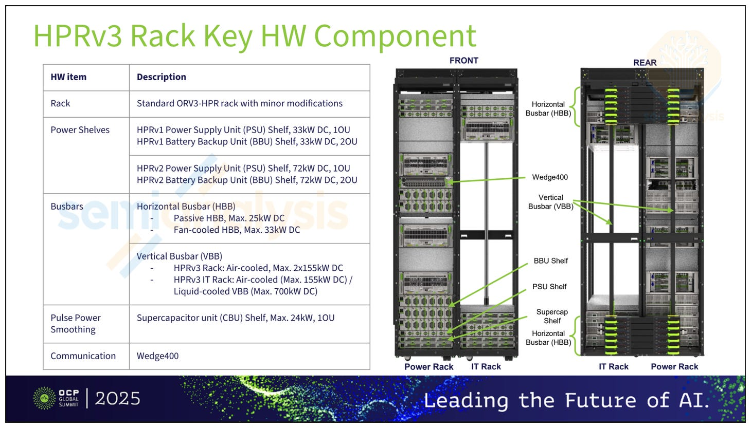
Meta's variant at OCP integrates additional power infrastructure into an adjacent rack rather than the compute rack itself. The auxiliary rack carries:
- BBU (Battery Backup Units) — short-duration battery support to ride through grid disturbances and brief outages.
- CBU (Capacitor Backup Units) — sub-second capacitor banks for peak shaving (absorbing transient power spikes from AI workloads without stressing the grid).
- Network switching — co-located in the same auxiliary rack for serviceability and density.
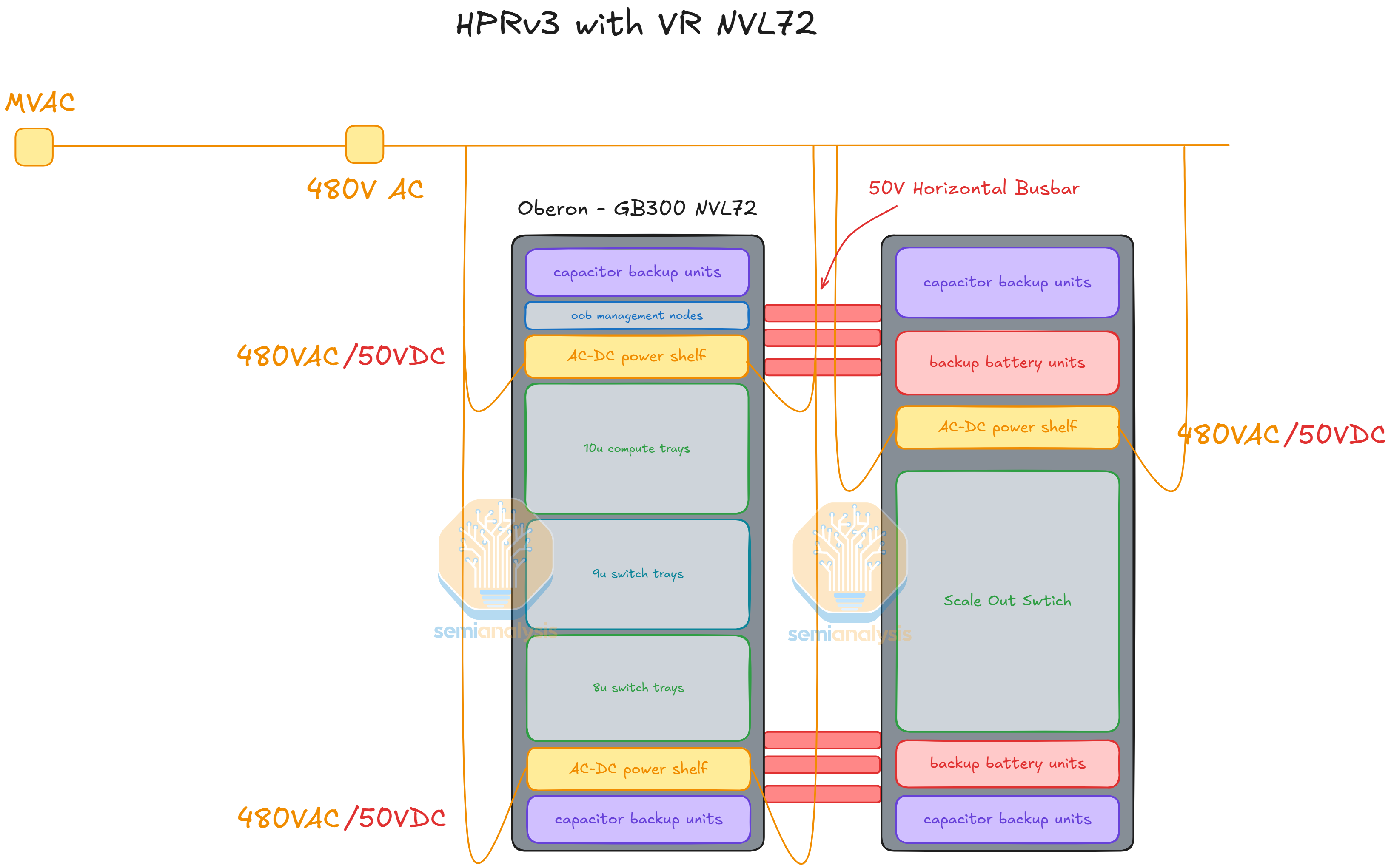
Why a separate rack? BBU and CBU shelves were too bulky to fit inside the GPU rack itself. Moving them to an adjacent rack gives Meta more energy-storage capacity than the GPU rack alone could host. The GPU rack and the high-power rack are connected via horizontal 50 V busbars.
3) Why Energy Storage Matters at This Scale
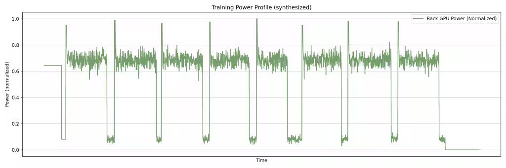
- AI training workloads generate bursty, highly synchronized power draws — every GPU in a cluster ramps simultaneously during forward-pass / backward-pass phases. These GPUs repeatedly move through the same training phases at nearly the same time. As a result, cluster-level power demand does not rise smoothly; it can spike sharply and simultaneously across many GPUs during compute- or communication-heavy steps.
- At rack-aggregate kW levels, these transients can stress utility grids and trigger protection circuits.
- CBU peak-shaving absorbs sub-second spikes locally. BBU bridging rides through longer events without dropping the workload.
- Together, they keep AI workloads from becoming a grid-stability problem.
4) Supplier Landscape
The rack-level power ecosystem — AC/DC conversion, 50 V vs 800 VDC distribution, BBU/CBU integration, liquid-cooled busbars, SST roadmap, and per-vendor commercial terms / timelines (Lite-On, Delta, Flex, Vertiv, Eaton, Advanced Energy, Hitachi Energy, GE Vernova, TE Connectivity, Amphenol) — is consolidated in Vera Rubin Decoded — Part 6 § 4 (Rack-Level Power Delivery).
For most non-hyperscaler buyers, the standard 4× 110 kW power-shelf reference design is what ships. HVDC and BBU/CBU rack architectures are predominantly hyperscaler customizations.
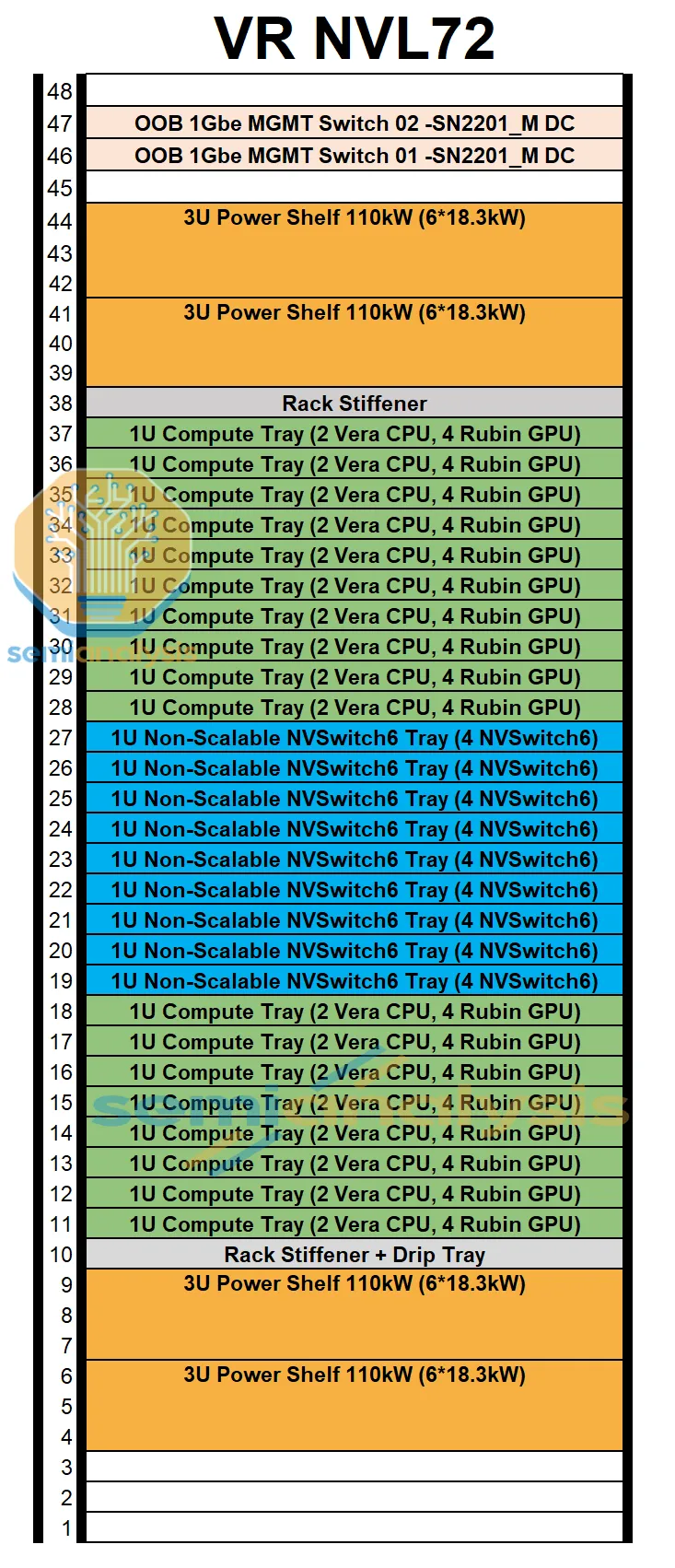
(10) Tray → Rack — How Trays Compose the VR NVL72 Rack
Working bottom-up: this section traces every internal lane inside a single compute tray, then shows how the trays connect to the NVLink switch trays at the center of the rack to form a single 72-GPU accelerator.
1) Rack-Level Overview
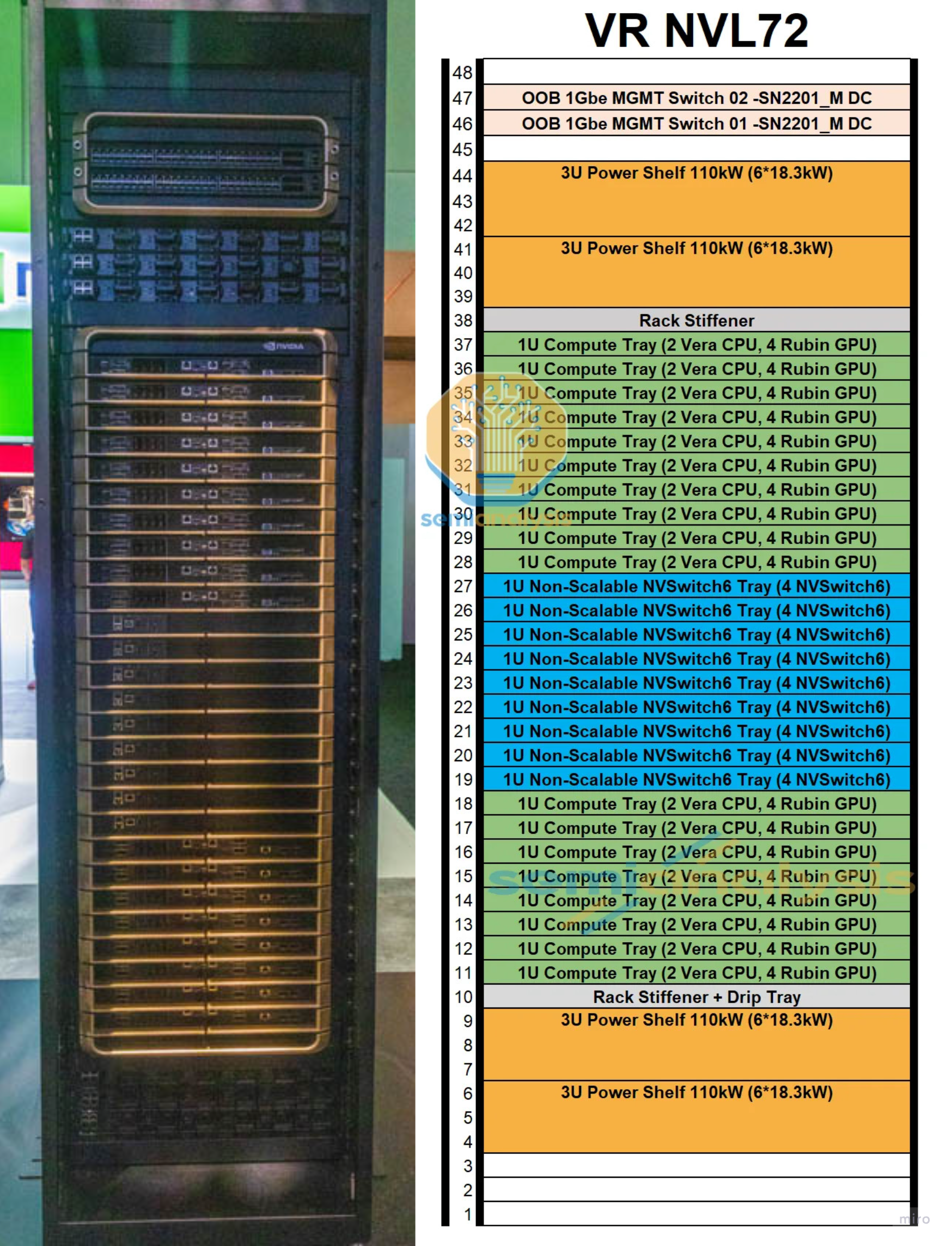
The rack stacks 18 compute trays + 9 NVLink switch trays + 4 power shelves into a single 19-inch cabinet:
- Each compute tray slots into the NVLink backplane at the back of the rack.
- The NVLink backplane is a separate physical layer from the compute-tray midplane — a passive copper backplane carrying NVLink 6 signals from each Strata module to the NVLink Switch Trays.
- The 9 switch trays (4 chips each = 36 NVLink 6 switch chips total) sit in the middle of the rack and connect every GPU to every other GPU in a full all-to-all topology.
- The 50 V liquid-cooled busbar runs vertically on one side of the rack, feeding every tray.
- The 4 power shelves — 2 at the top of the rack (U41–44) and 2 at the bottom (U4–9) — feed the busbar from both ends.
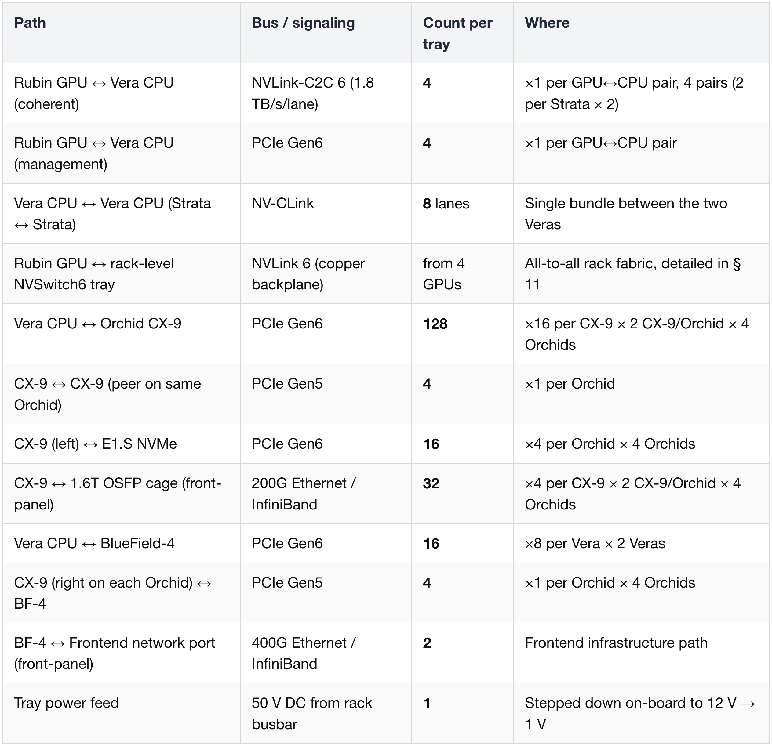
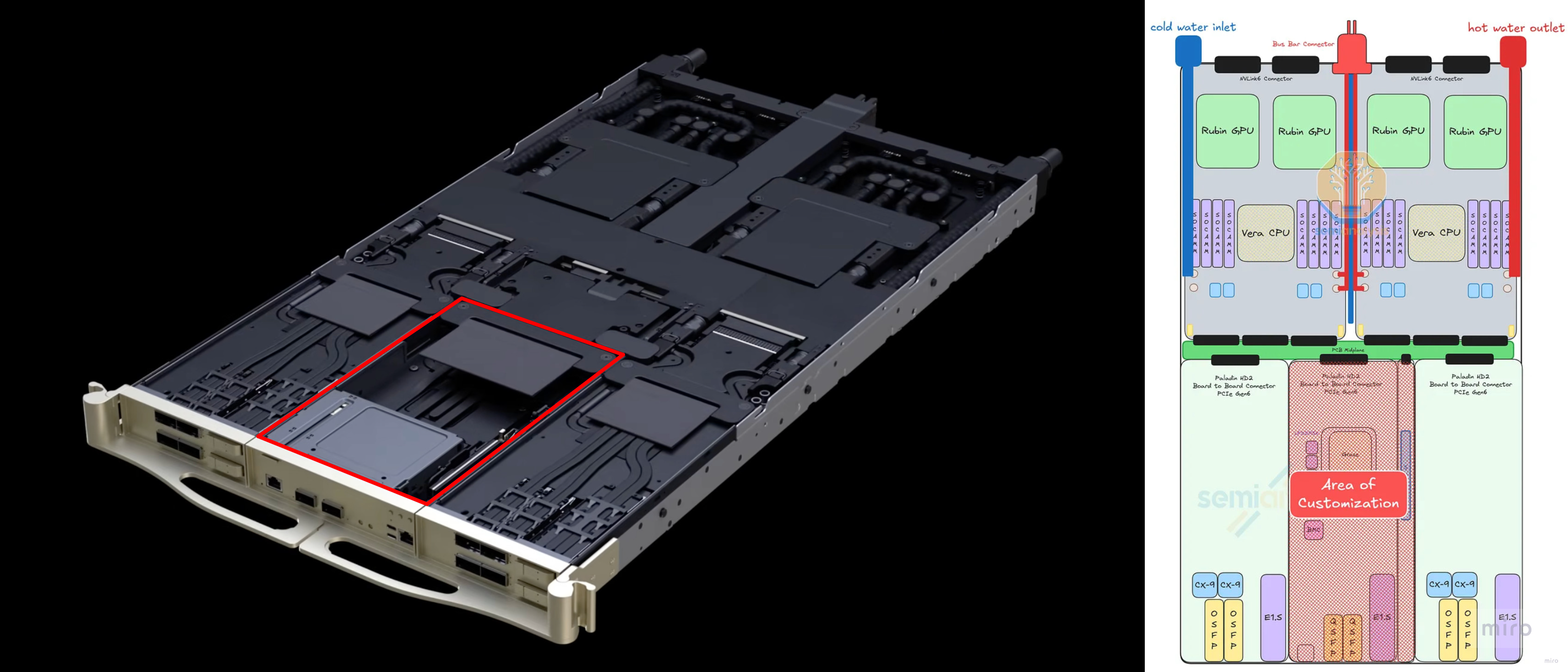
2) Inside a Single Compute Tray (1U · 2 Vera CPUs + 4 Rubin GPUs)
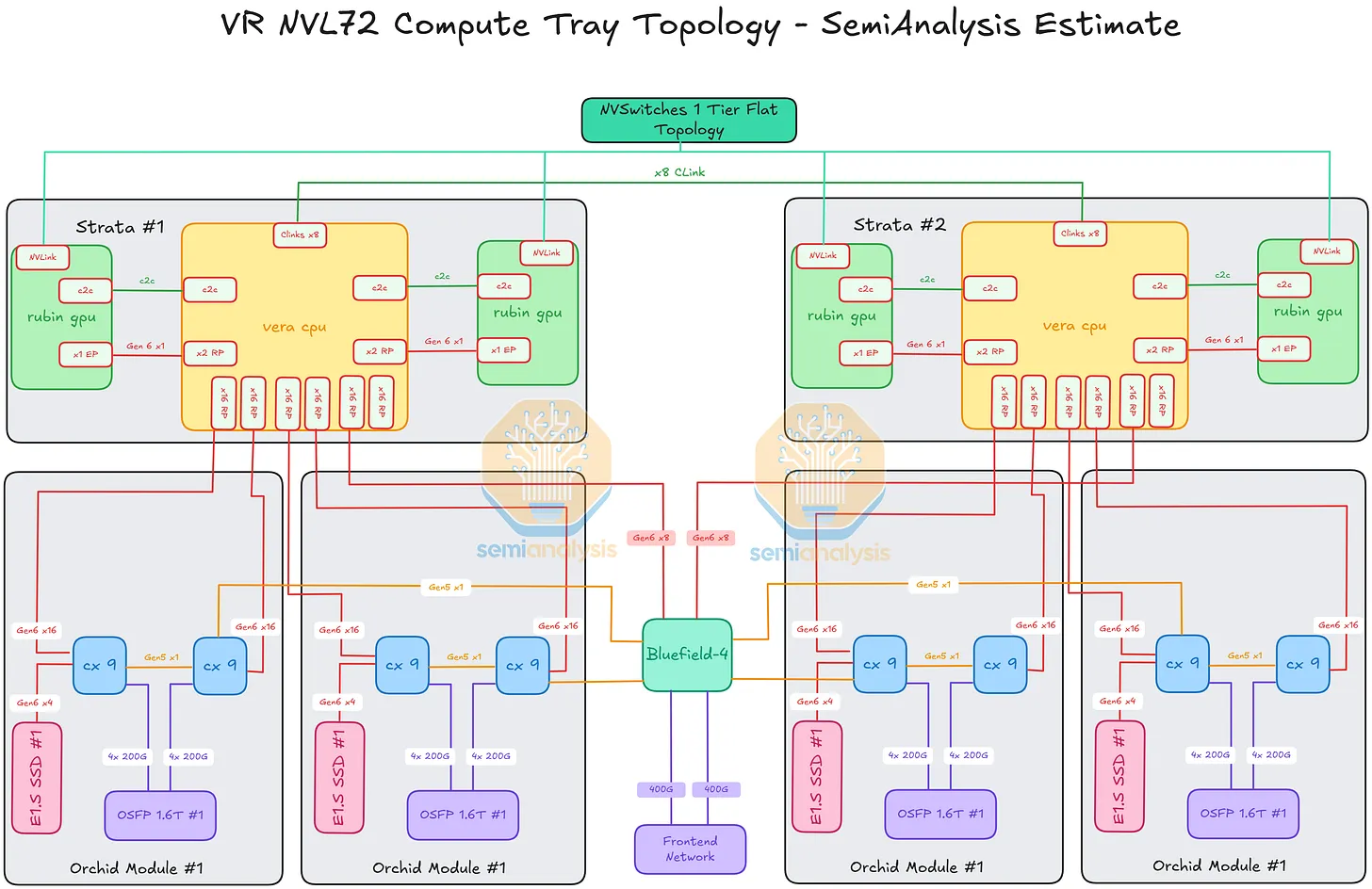
The lane-by-lane wiring inside one compute tray. Reading from the Strata modules outward:
Inside One Strata Module — Rubin GPU ↔ Vera CPU ↔ Rubin GPU
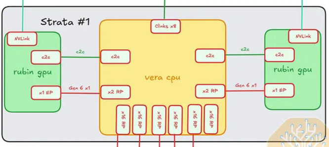
Each Strata module holds 1 Vera CPU + 2 Rubin GPUs. Each Rubin is connected to the Vera through two parallel paths:
- NVLink-C2C (coherent path): ×1 NVLink 6 C2C lane per GPU↔CPU pair — carries coherent memory traffic at 1.8 TB/s
- PCIe path: ×1 PCIe Gen6 lane per GPU↔CPU pair — management / secondary I/O
There are 2 such GPU↔CPU pairs per Strata module (one per Rubin GPU).
Between the Two Strata Modules — Vera CPU ↔ Vera CPU
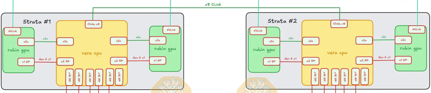
The two Vera CPUs (one per Strata) are tied together so the tray operates as a single coherent compute domain:
- Vera ↔ Vera: ×8 NV-CLink lanes
Rubin GPUs ↔ NVLink Switch Trays (rack-scale path)
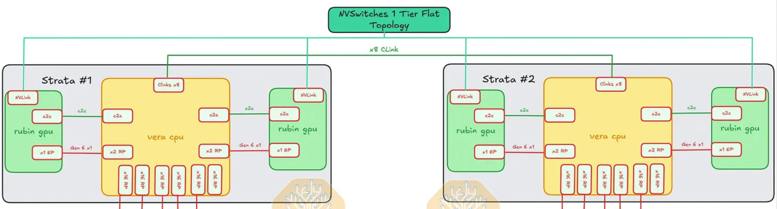
Each Rubin GPU also connects directly out of the tray into the rack-level NVLink fabric:
- Rubin GPU ↔ NVSwitch: NVLink 6 GPU-to-GPU lanes via the NVLink backplane at the back of the rack
- This is the all-to-all rack-scale path — full topology covered in § 11.
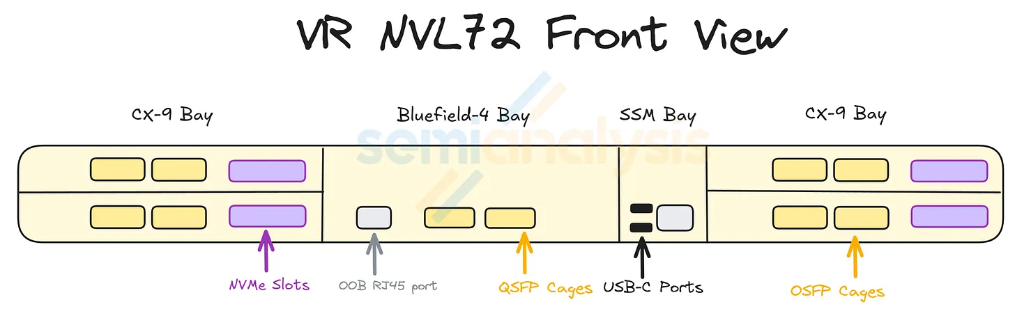
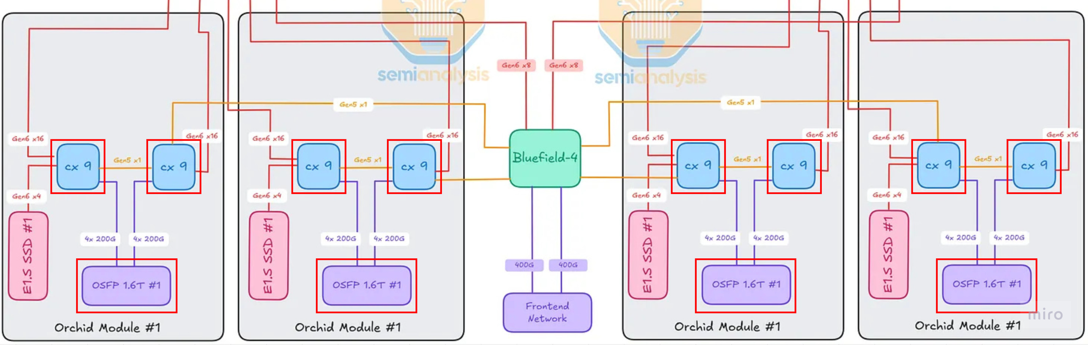
Vera CPU ↔ Orchid Module (scale-out networking + local storage)
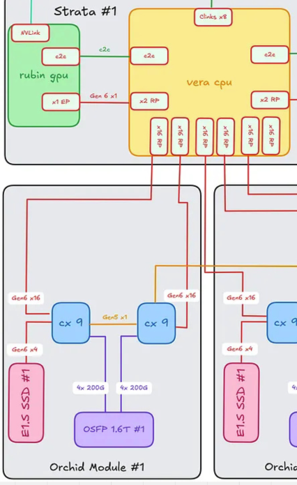
Each tray has 4× Orchid modules, each carrying 2× ConnectX-9 (CX-9) NICs. Per Orchid module:
- Vera ↔ CX-9: ×16 PCIe Gen6 lanes per CX-9 (×32 lanes total across both CX-9s on the module)
- CX-9 ↔ CX-9 (peer link): ×1 PCIe Gen5 lane between the two CX-9 cards on the same Orchid
- Left-side CX-9 ↔ E1.S NVMe SSD slot: ×4 PCIe Gen6 lanes
- CX-9 ↔ 1.6T OSFP cage (scale-out network): ×4 200G Ethernet/InfiniBand lanes per CX-9 (×8 total per Orchid)
Lane totals to/from a single Orchid module:
- ×36 PCIe Gen6 lanes (×32 to the two CX-9s + ×4 to E1.S SSD)
- ×1 PCIe Gen5 lane (CX-9 peer link)
- ×8 200G Ethernet / InfiniBand lanes (front-panel scale-out)
Vera CPU ↔ BlueField-4 Module (frontend infrastructure plane)
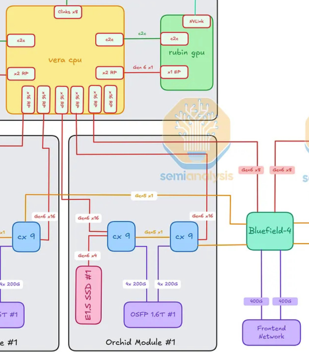
The BF-4 module is the third major destination off the Vera CPUs. The connections going into and out of BF-4:
- Vera ↔ BF-4: ×8 PCIe Gen6 lanes per Vera (×16 lanes total — one Vera per Strata × 2 Stratas)
- CX-9 (right-side on each Orchid) ↔ BF-4: ×1 PCIe Gen5 lane per CX-9 (×4 lanes total across the 4 Orchids)
- BF-4 ↔ Frontend Network port: ×2 400G Ethernet/InfiniBand lanes
Lane totals to/from the BF-4 module:
- ×16 PCIe Gen6 lanes (from the two Veras)
- ×4 PCIe Gen5 lanes (from the 4 Orchids' right-side CX-9s)
- ×2 400G Ethernet / InfiniBand lanes (frontend network)
Single VR NVL72 Compute Tray — Module & Lane Summary
Modules per tray:
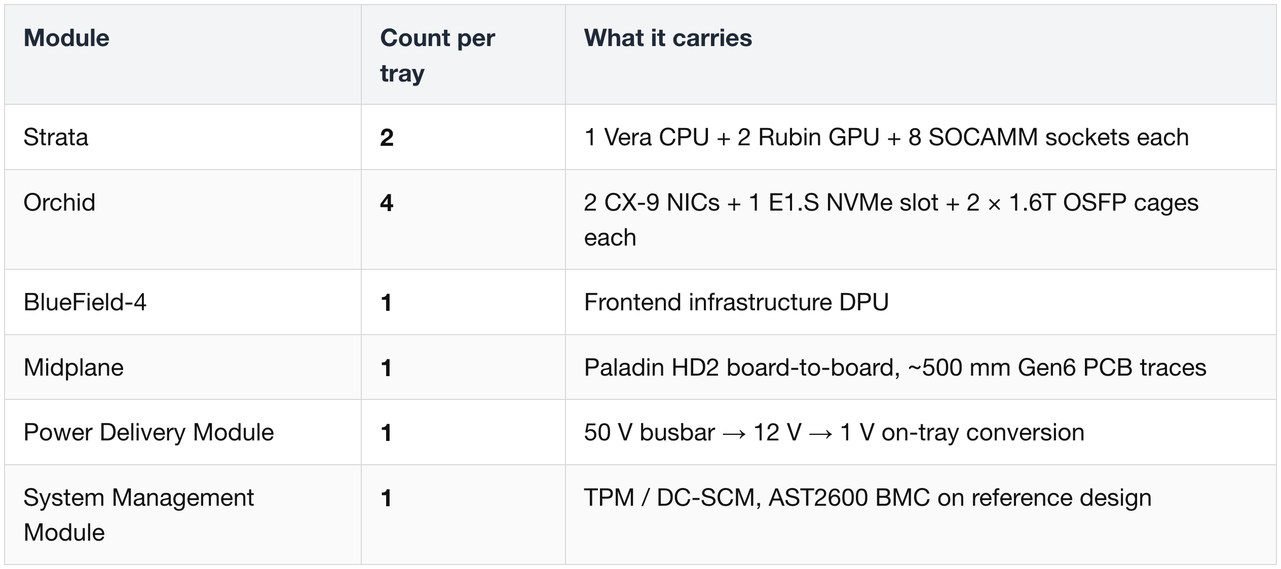
Lane counts per tray (totals across all modules):
Front-panel external connectivity per tray: 8 × 1.6T OSFP cages (scale-out) + 1 × frontend port (BF-4 400G ×2 lanes) + 1 × BMC/management.
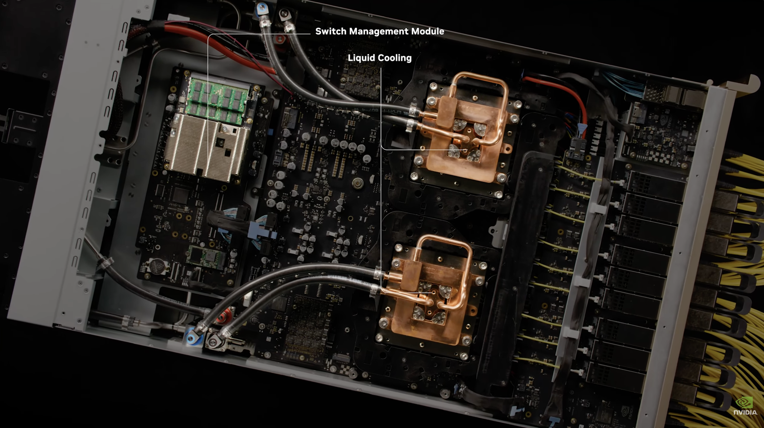
3) NVLink Switch Tray — Where Compute Trays Meet
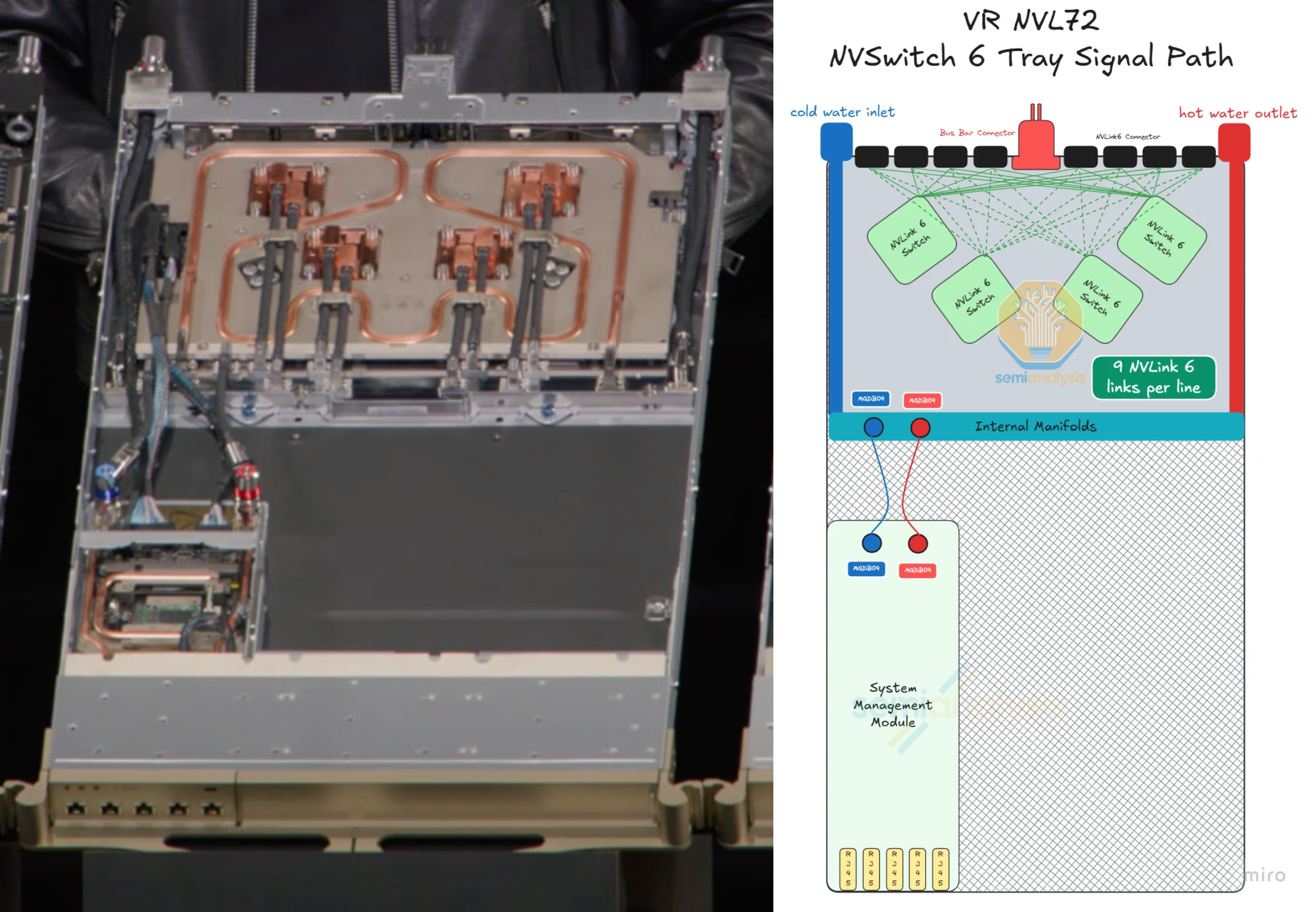
Compute trays connect into the NVLink switch trays at the center of the rack via the NVLink 6 copper backplane. Each switch tray houses 4× NVLink 6 Switch chips on a single PCB.
Inside the switch tray
- The NVLink 6 Switch board is liquid-cooled, covered with a single cold-plate module.
- The tray hosts a System Management Module (SMM) with its own CPU acting as the host to the switch tray.
- The SMM ↔ switch tray connection uses flyover cables — the only flyover cable connection in the entire VR NVL72 system. This carve-out is acceptable because (a) the PCIe link to the SMM is lower speed, and (b) the switch tray contains relatively few modules, so it doesn't recreate the assembly-failure pattern that drove the rest of the system to a cableless design.
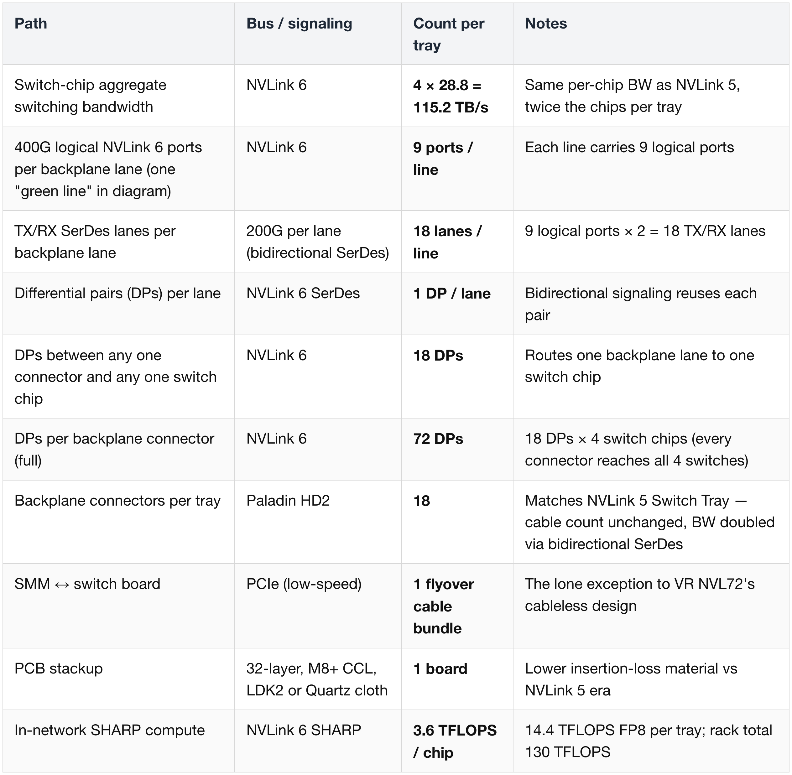
Backplane lane structure
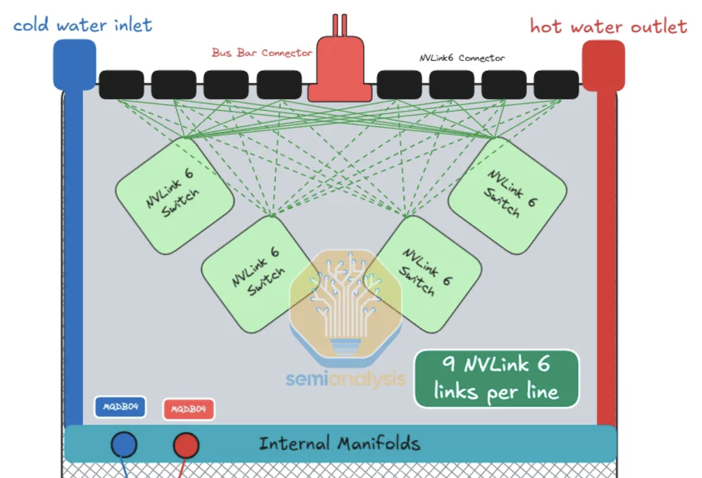
- Each green line in the diagram represents 9× 400G logical NVLink 6 ports, or equivalently 18× TX/RX lanes at 200G.
- Because NVLink 6 uses bidirectional SerDes, there is 1 differential pair (DP) per lane → 18 DPs between any connector and any switch, 72 DPs per connector total
- Cable count per connector matches the prior NVLink 5 Switch Tray — the doubling of bandwidth comes entirely from bidirectional signaling, not from more copper.
Switch-tray PCB upgrade
- Bidirectional signaling on NVLink 6 has much lower tolerance for insertion loss than NVLink 5.
- The dense routing between Amphenol PaladinHD2 connectors and the NVLink Switch chips adds further PCB complexity.
- The NVLink 6 Switch board PCB is upgraded to 32 layers with M8+ grade CCL, using LDK2 glass fiber cloth at minimum (possibly Quartz fiber cloth) — the same material story that drives the compute-tray PCB upgrade in § 5.
Single NVSwitch6 Tray — Module & Lane Summary
Modules per switch tray:
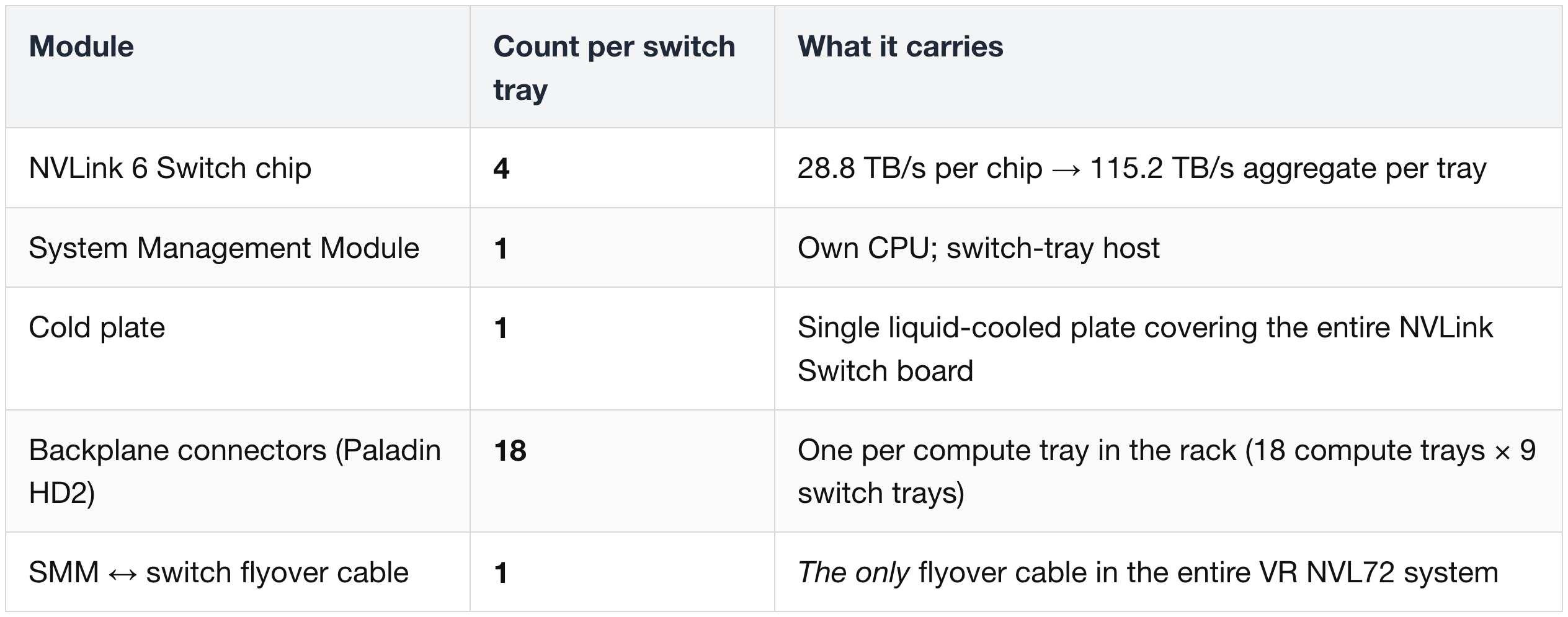
Lane counts per switch tray:
Aggregate at the rack level: 9 NVSwitch6 trays × 4 chips = 36 NVLink 6 Switch chips per VR NVL72, delivering ~260 TB/s all-to-all bandwidth across the 72 Rubin GPUs.
4) What Lives at Each Layer (recap)
- Inside the Strata module: Rubin ↔ Vera via NVLink-C2C (coherent) + PCIe Gen6 (management).
- Inside the tray (Strata ↔ Strata): Vera ↔ Vera via ×8 NV-CLink lanes.
- Inside the tray (Strata ↔ front modules): PCIe Gen6 + PCIe Gen5 traverse the Midplane to reach Orchid, BF-4, PDB, and Mgmt modules.
- Tray ↔ rack-level fabric: NVLink 6 over the copper backplane to the NVLink Switch Trays.
- Outside the rack: 200G / 400G Ethernet or InfiniBand via CX-9 (scale-out) and via BF-4 (frontend).
(11) Scale-Up Network — NVLink 6 Inside the Rack
The scale-up network is what makes the rack "act as one accelerator". Inside the VR NVL72 rack, all 72 Rubin GPUs talk to each other through the rail-optimized all-to-all NVLink 6 fabric.
Rail-optimized — what it means
Each GPU's NVLink 6 bandwidth (3.6 TB/s bidirectional) is not one fat pipe to one switch. It's split into multiple parallel "rails" — independent NVLink lanes — that each connect to a different NVLink 6 switch chip.
- A given GPU sends data simultaneously across its rails, with each rail going to a different switch.
- The receiving GPU pulls data through its own rails coming back from those same switches.
- This is the same rail-optimized pattern Nvidia used in GB200 NVL72 with NVLink 5, just doubled in per-rail rate.
All-to-all — every GPU connects to every switch
- 72 GPUs × 36 NVLink 6 switch chips are wired such that every GPU has at least one rail to every switch chip in the rack.
- Consequence: every GPU-to-GPU path is one switching hop. No leaf-spine hierarchy inside the rack.
- This is why MoE workloads scale well — the expert-dispatch all-to-all collective doesn't have to route around domain boundaries.
Physical wiring — the backplane
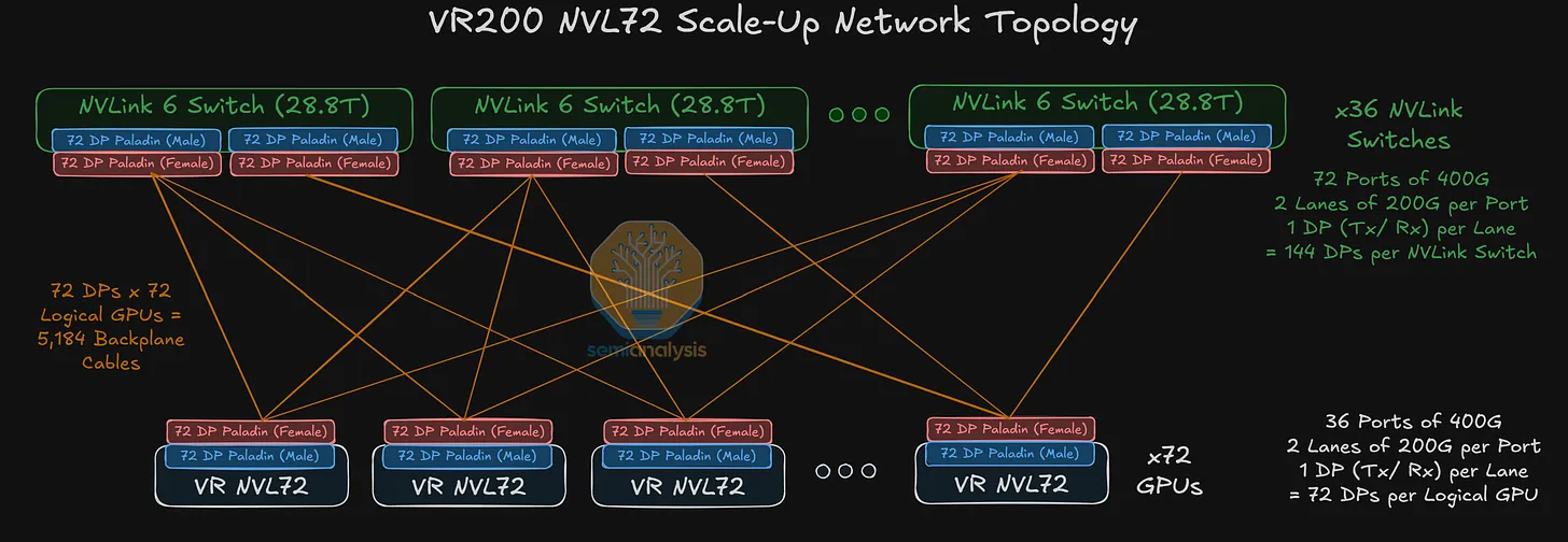
- The 72 GPUs and 36 switch chips are connected via the NVLink 6 copper backplane at the back of the rack.
- The backplane carries approximately 5,000 copper cables, identical cable count as GB300 thanks to bidirectional SerDes — covered in Vera Rubin Decoded — Part 3 § 5 (NVLink 6 Switch).
- Maximum cable reach is at least 1 m, which is what lets the bidirectional signaling stay reliable across the full rack height.
- Amphenol supplies the PaladinHD2 backplane connectors that terminate every cable into both the Strata modules and the NVLink Switch Trays.
What stays unchanged vs GB200/GB300
- Cable count — same ~5,000 copper cables
- Connector layout — same PaladinHD2 backplane connectors from Amphenol
- Topology — still flat all-to-all, still rail-optimized
- Rack form factor — same 19-inch Oberon chassis
What changes
- Per-link rate doubles (200G → 400G effective via bidirectional signaling)
- Per-GPU bandwidth doubles (1.8 TB/s → 3.6 TB/s)
- Per-rack switch chip count doubles (18 → 36, organized as 9 trays × 4 chips)
Why scale-up stays inside the rack
Beyond ~1 m of copper reach, signal integrity degrades enough that the bidirectional SerDes can't hold timing. So NVLink 6 stays inside the rack — any GPU-to-GPU traffic that needs to cross racks has to leave the NVLink fabric and travel through ConnectX-9 + InfiniBand or Ethernet (the scale-out fabric in the next sections). This is the canonical "scale-up vs scale-out" boundary.
(12) Scale-Out — InfiniBand Networks (Nvidia Quantum-X)
Once GPU traffic leaves the rack, Nvidia offers two parallel AI networking platforms — one for each protocol family:
The "-X" suffix doesn't mean the same protocol on both — it means "next-gen, photonics-enabled" version of the platform for each network family. Quantum-X = InfiniBand; Spectrum-X = Ethernet. This section (§ 12) covers Quantum-X. § 13 covers Spectrum-X, plus the non-Nvidia Ethernet alternatives that compete with it.
Both platforms are optics-based at scale-out distances. Every NIC↔switch and switch↔switch link in either family rides on optical fiber, in pluggable transceiver form on the non-CPO SKUs (Q3400, SN6600) or as co-packaged optics on the photonics SKUs (Q3450, SN6810, SN6800).
Copper SerDes can't sustain 800G signal integrity much beyond ~1 m, so once GPU traffic leaves the rack's NVLink copper backplane (§ 11), the next hop must be optical. This is why the optics ecosystem — transceiver suppliers, fiber routing, CPO maturity — matters as much as the switch silicon for scale-out economics.
Components & high-level architecture of the Quantum X800 Q3450 Switch — zooming outside-in across three movements: (1) where it lives in the rack, (2) what it is as a unit, (3) what's inside, from silicon to fiber to front-panel cages.
1) Where it lives — rack deployment context
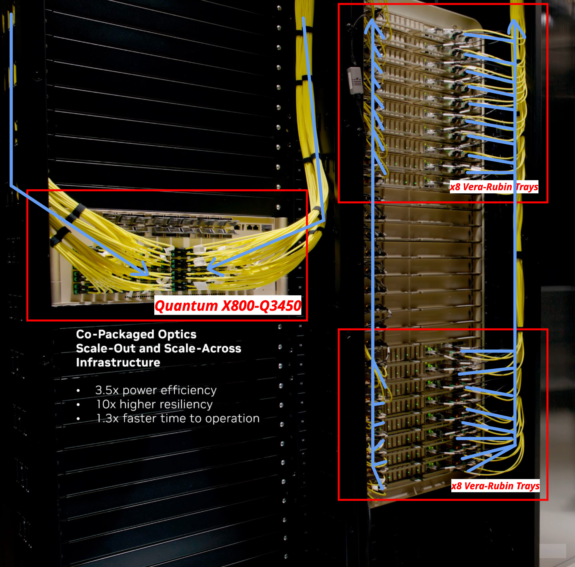
Q3450 sits in the scale-out switch row, fanning yellow MPO fiber bundles into stacks of Vera-Rubin trays.
2) The switch as a unit — headline specs in one frame
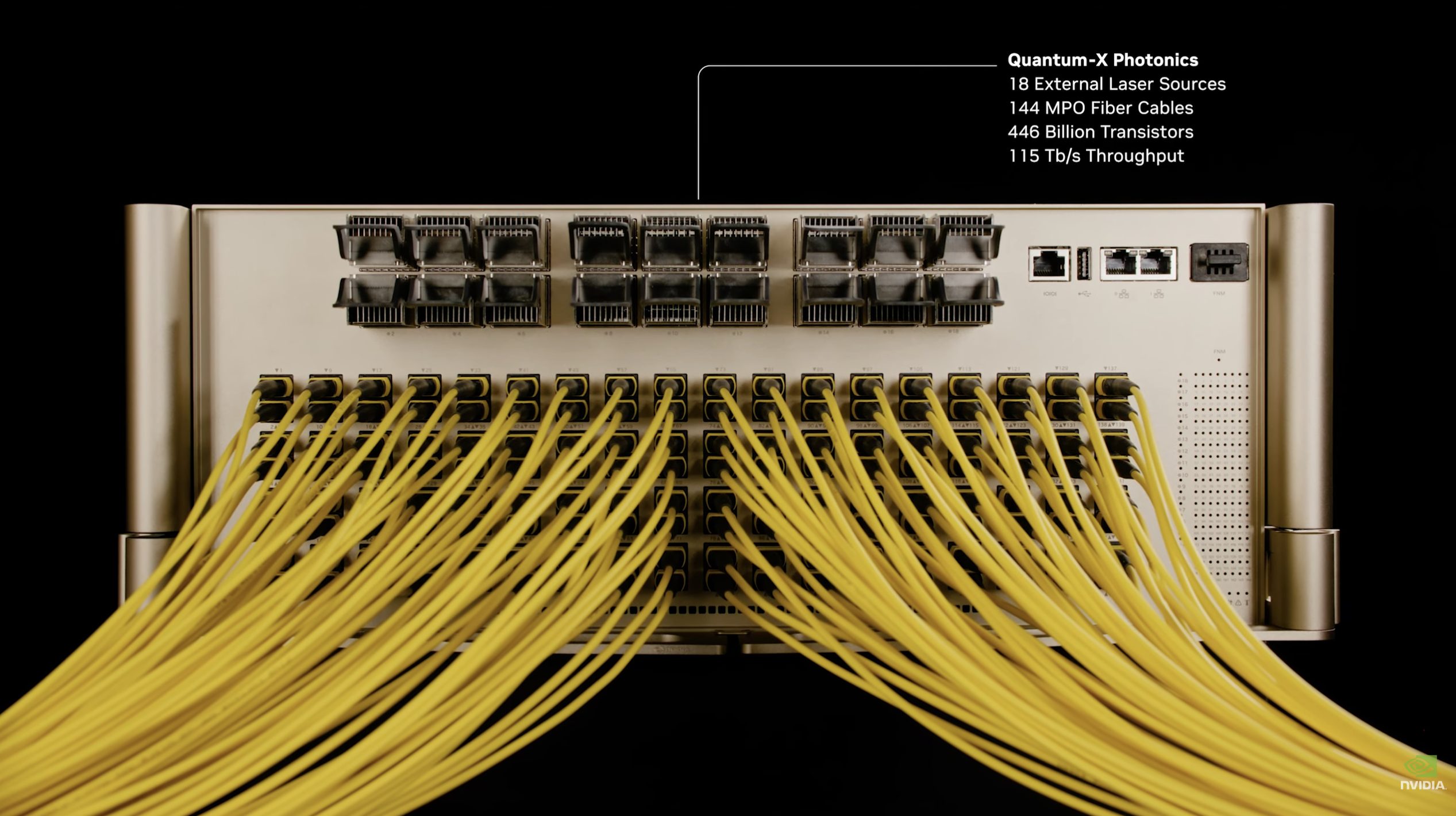
18 ELS modules on the top row, 144 MPO fiber-cable cages on the bottom row, 446 billion transistors across the 4 internal ASICs, 115 Tb/s aggregate throughput.
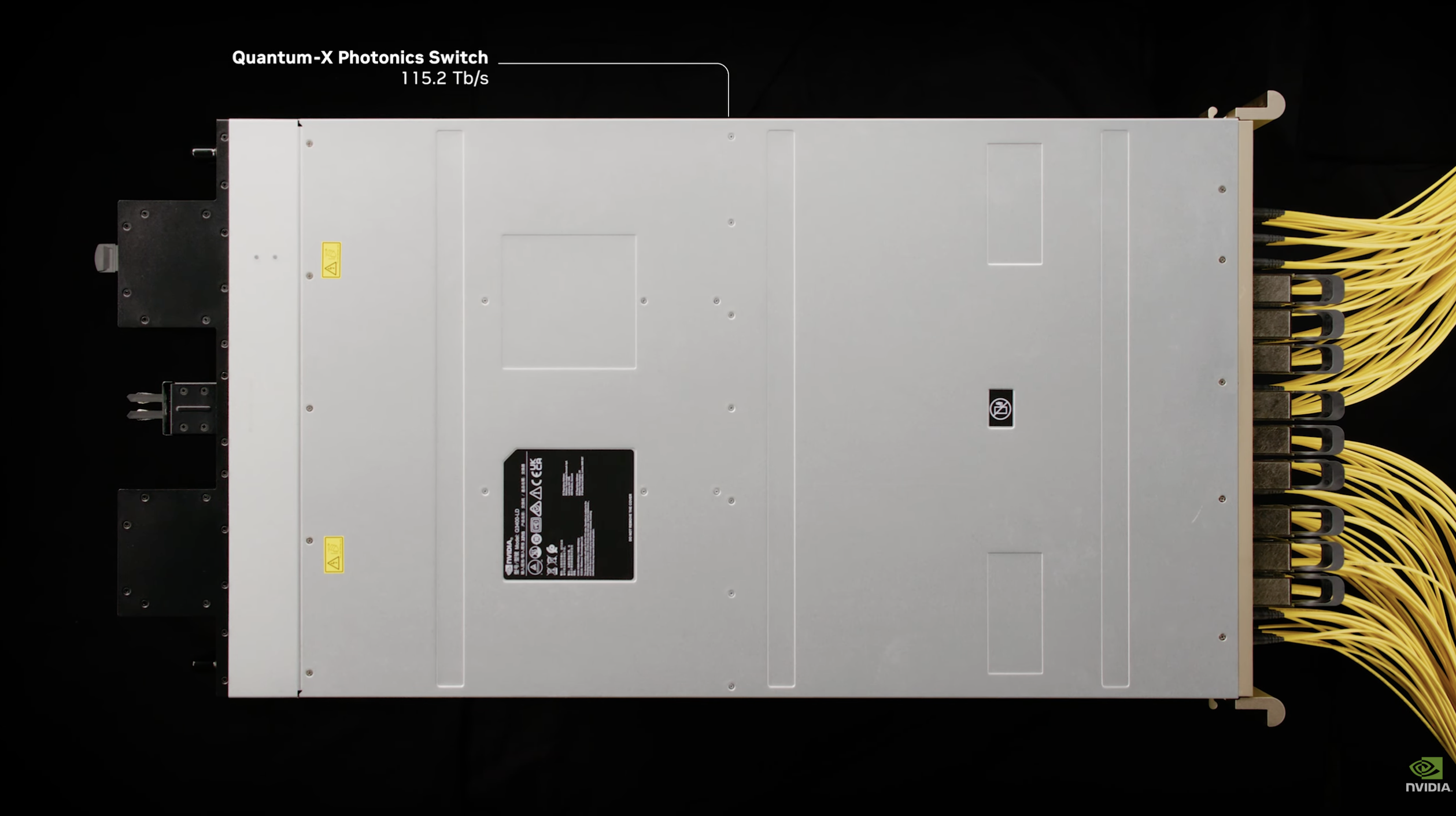
Chassis top-down view. Yellow MPO fibers exit the right side; service access from the top.
3) Inside — lid off, board level
Lid off. SMM and BMC on the left; the two copper cold-plate blocks cover the photonic packages. Coolant inlet/outlet routed from the top.
4) Inside — Photonic Package (silicon zoom · level 1)
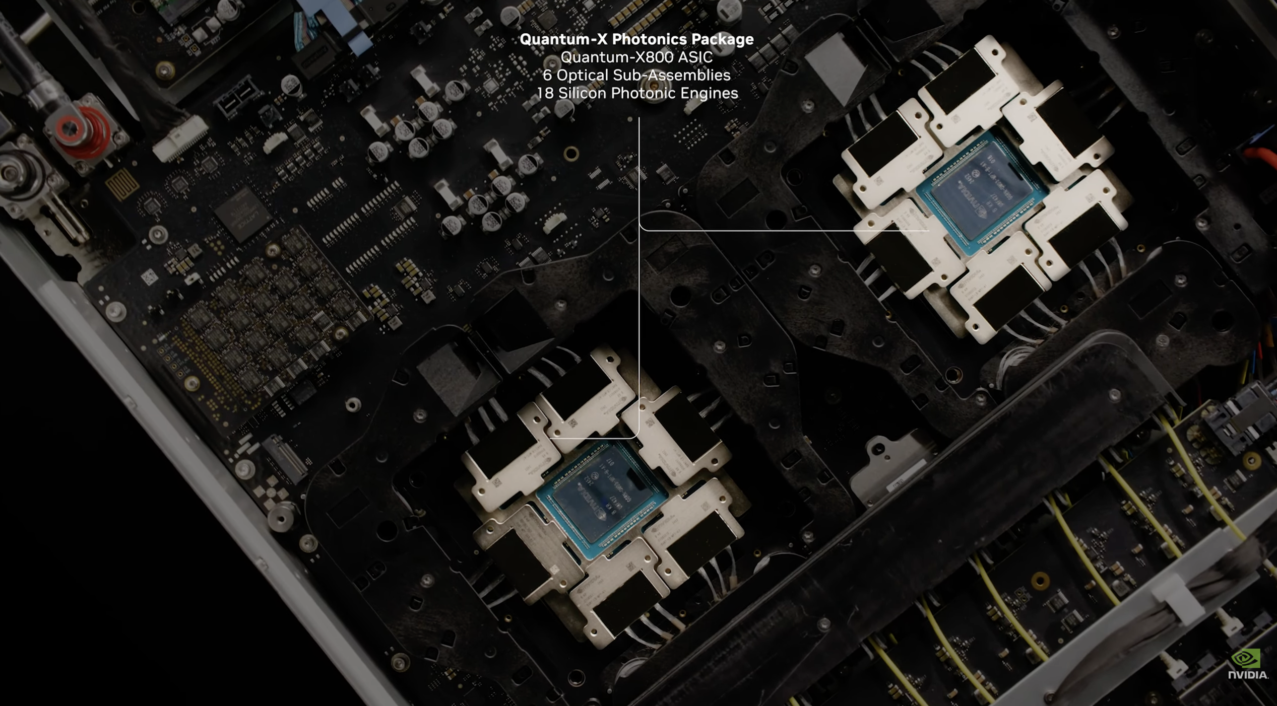
Cold plates removed. The Q-X800 ASIC sits at the center; 6 Optical Sub-Assemblies (OSAs) ring it. 18 Silicon Photonic Engines total — 3 per OSA.
5) Inside — Detachable Optical Sub-Assembly (silicon zoom · level 2)
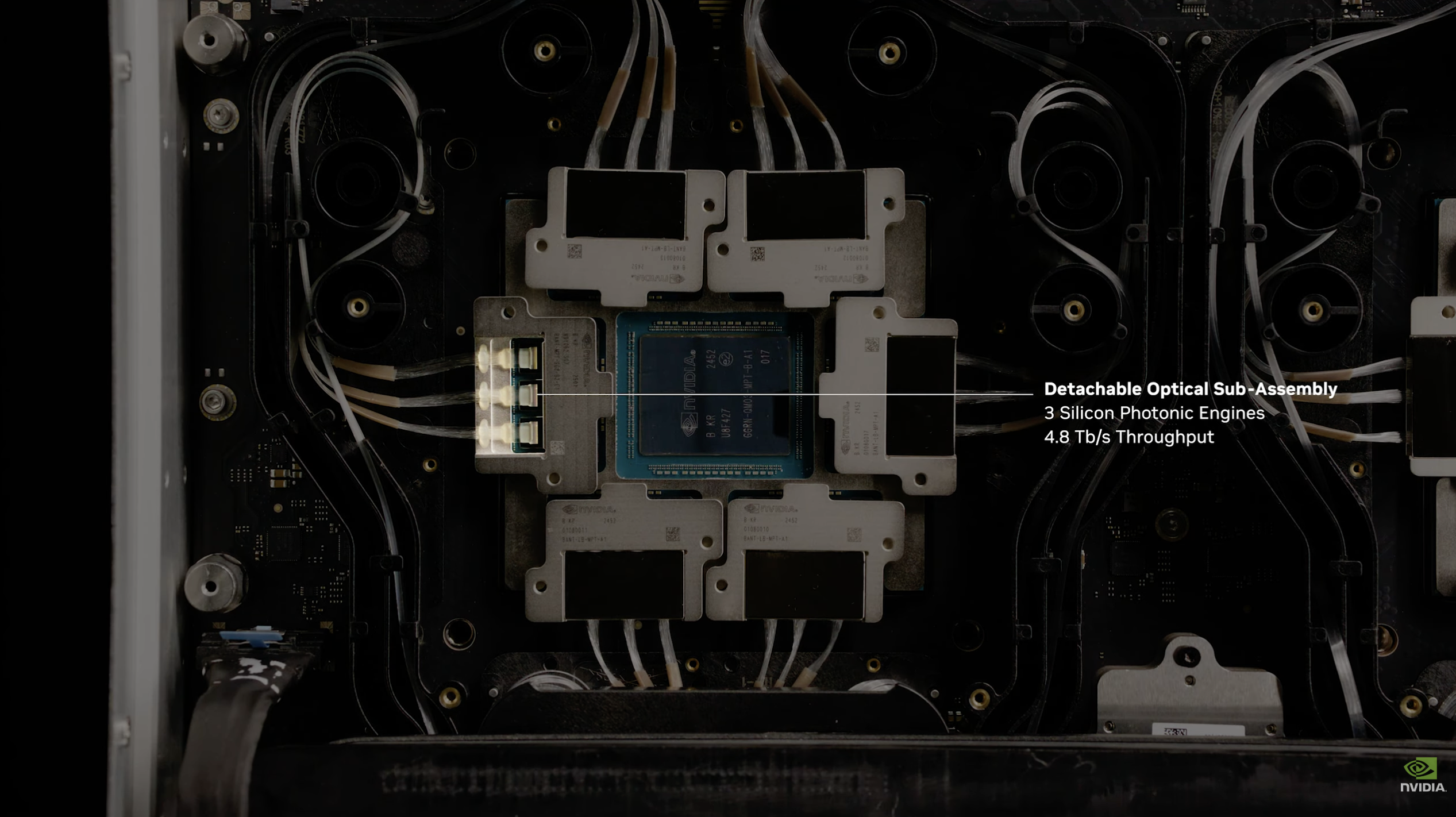
One OSA detached from the package. 3 Silicon Photonic Engines per assembly · 4.8 Tb/s. Field-replaceability is the operational rationale for the detachable form factor.
6) Inside — Single Silicon Photonic Engine (silicon zoom · level 3)
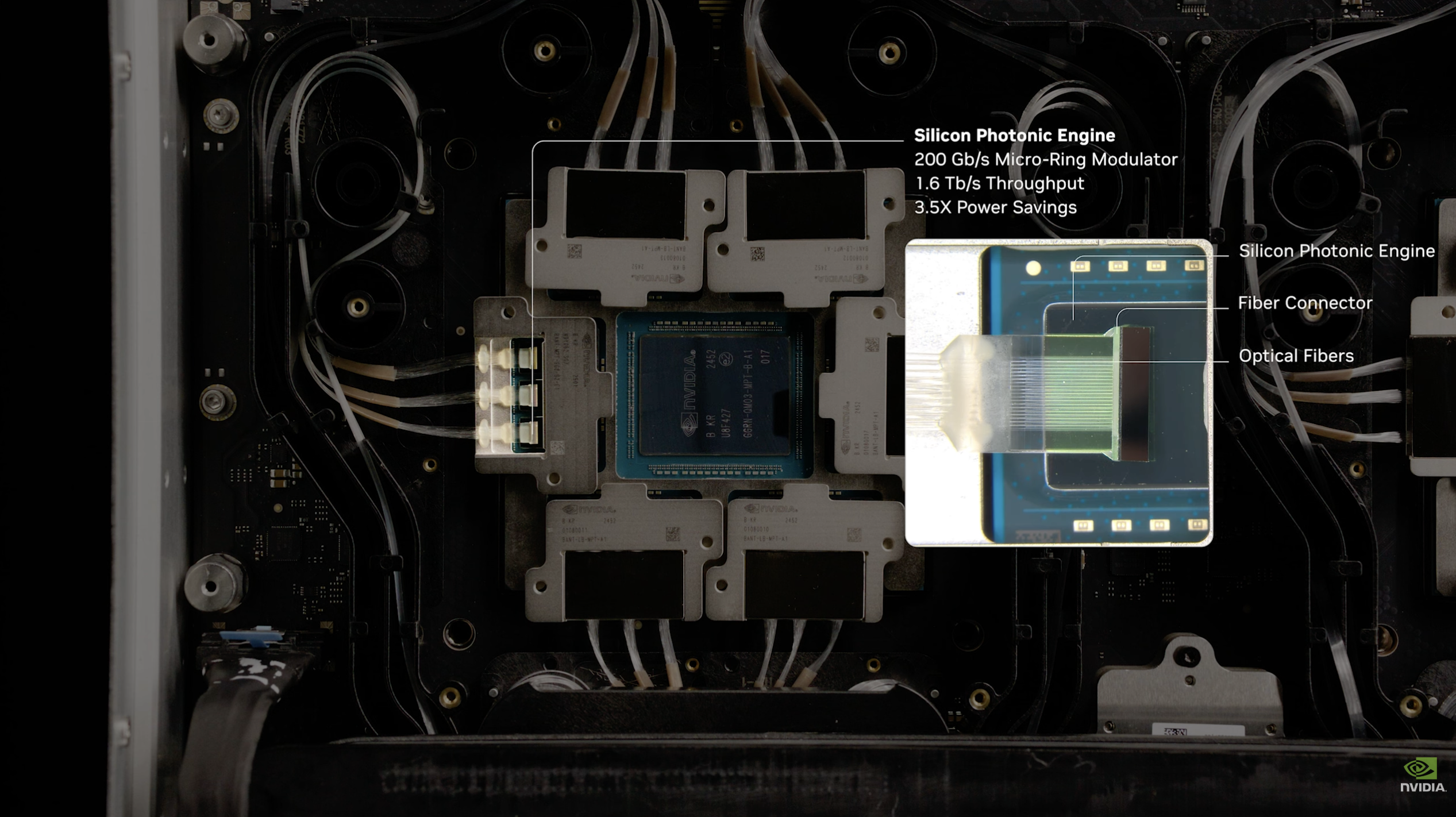
One SPE. 200 Gb/s Micro-Ring Modulator (MRM) · 1.6 Tb/s per engine · 3.5× power savings vs equivalent pluggable transceivers. This is what CPO actually substitutes for.
7) Inside — the 324 optical connections, summarized
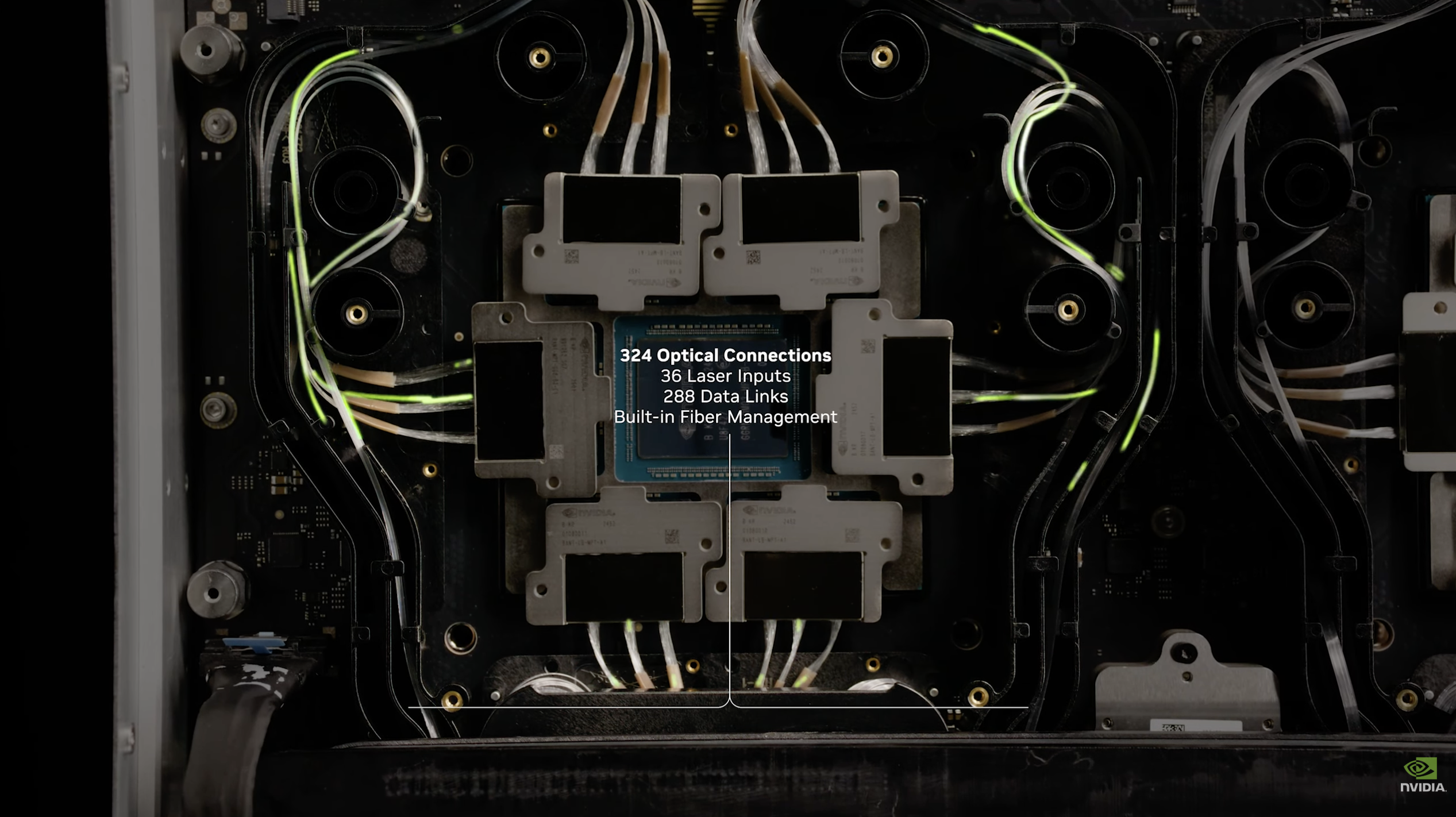
The connection-count summary. 324 = 36 laser inputs (from the 18 ELS modules) + 288 data links (from the 18 SPEs). All routed through built-in fiber management — no external fiber harnesses required.
8) Inside — internal fiber routing
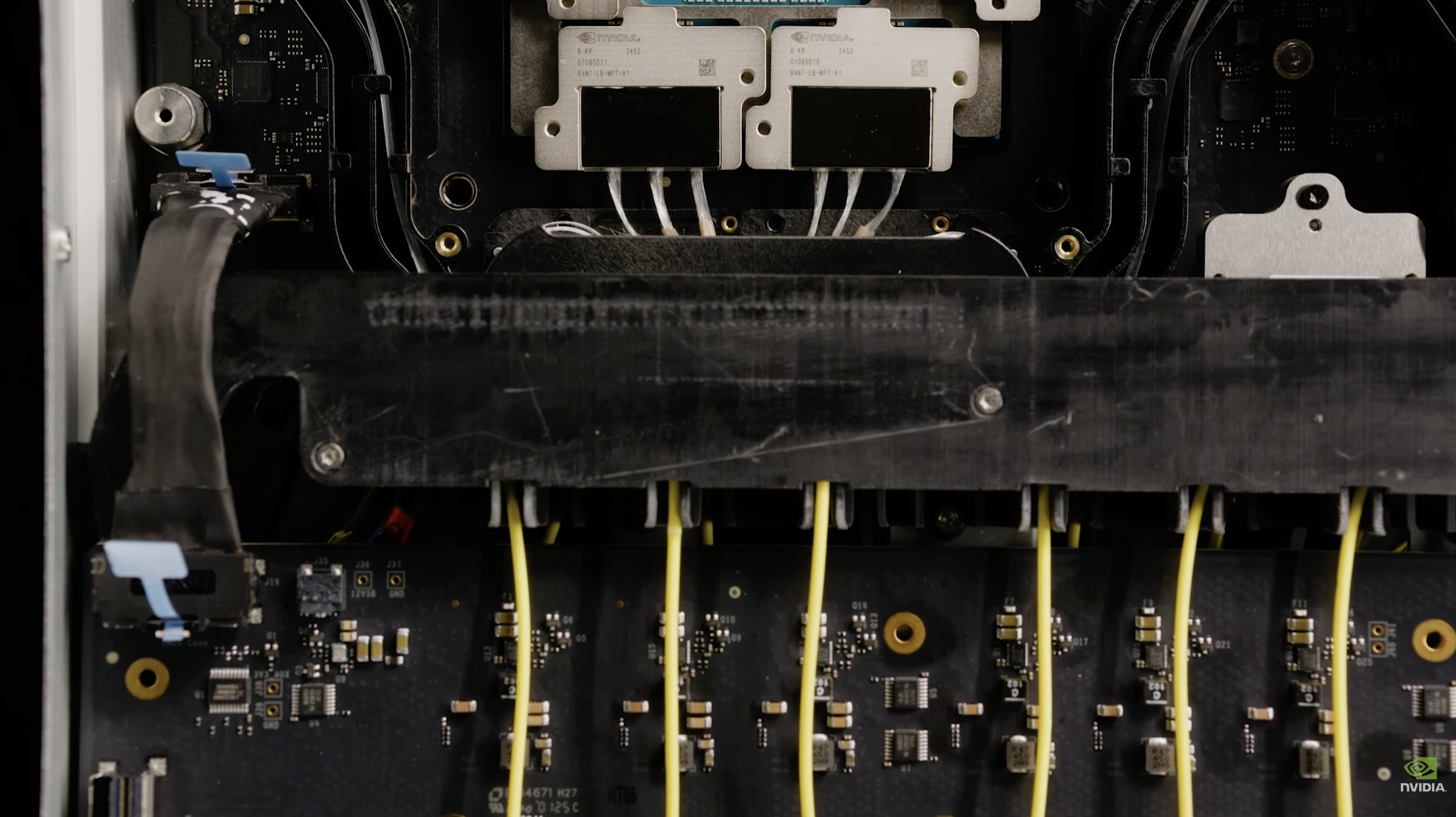
Fiber harness routing across the board floor. Black ribbon carrier hides the bulk of the SMF runs; yellow strain-relief boots terminate at the MMC connector array.
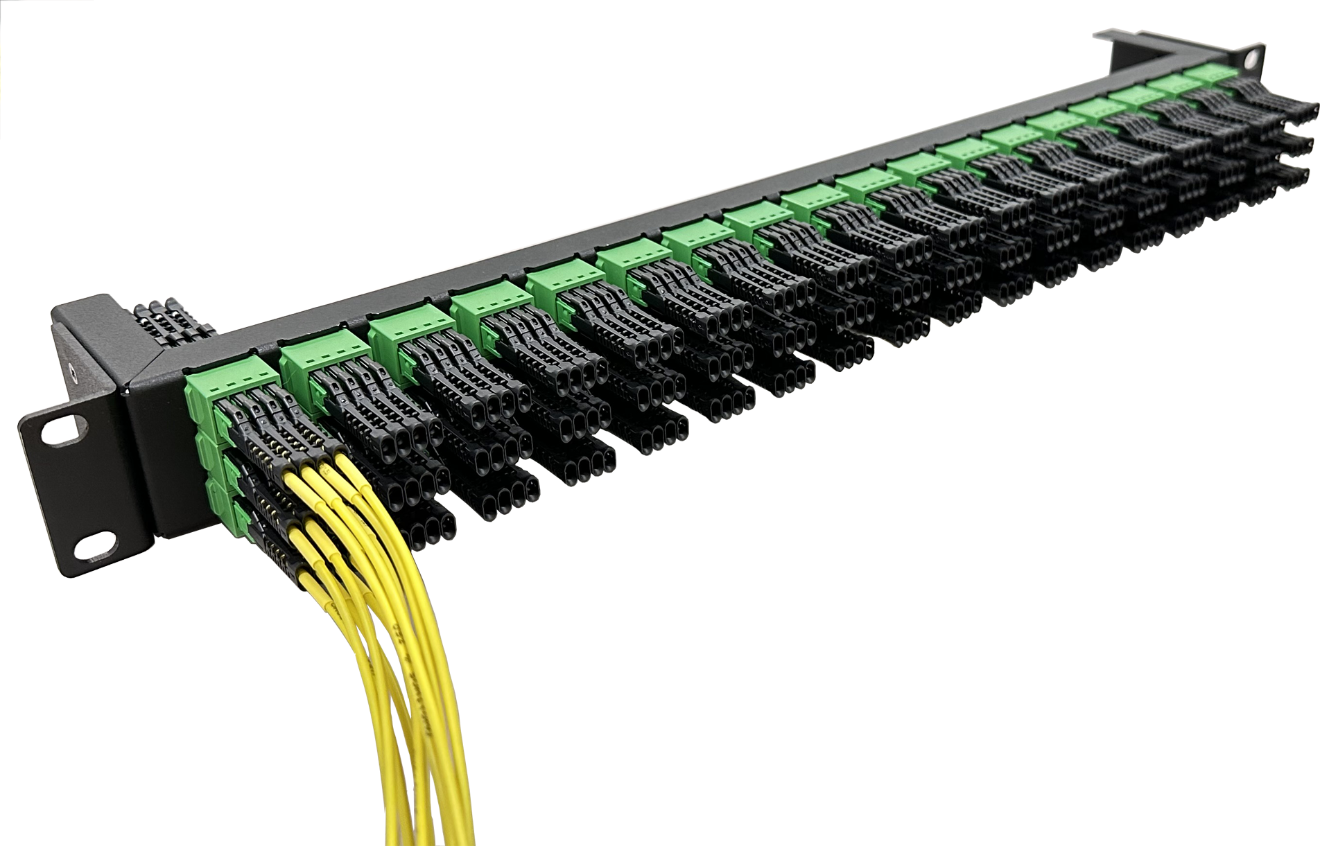
This is what an MMC connector looks like (Product of Sumitomo Electric).
9) Inside — External Laser Source (ELS)
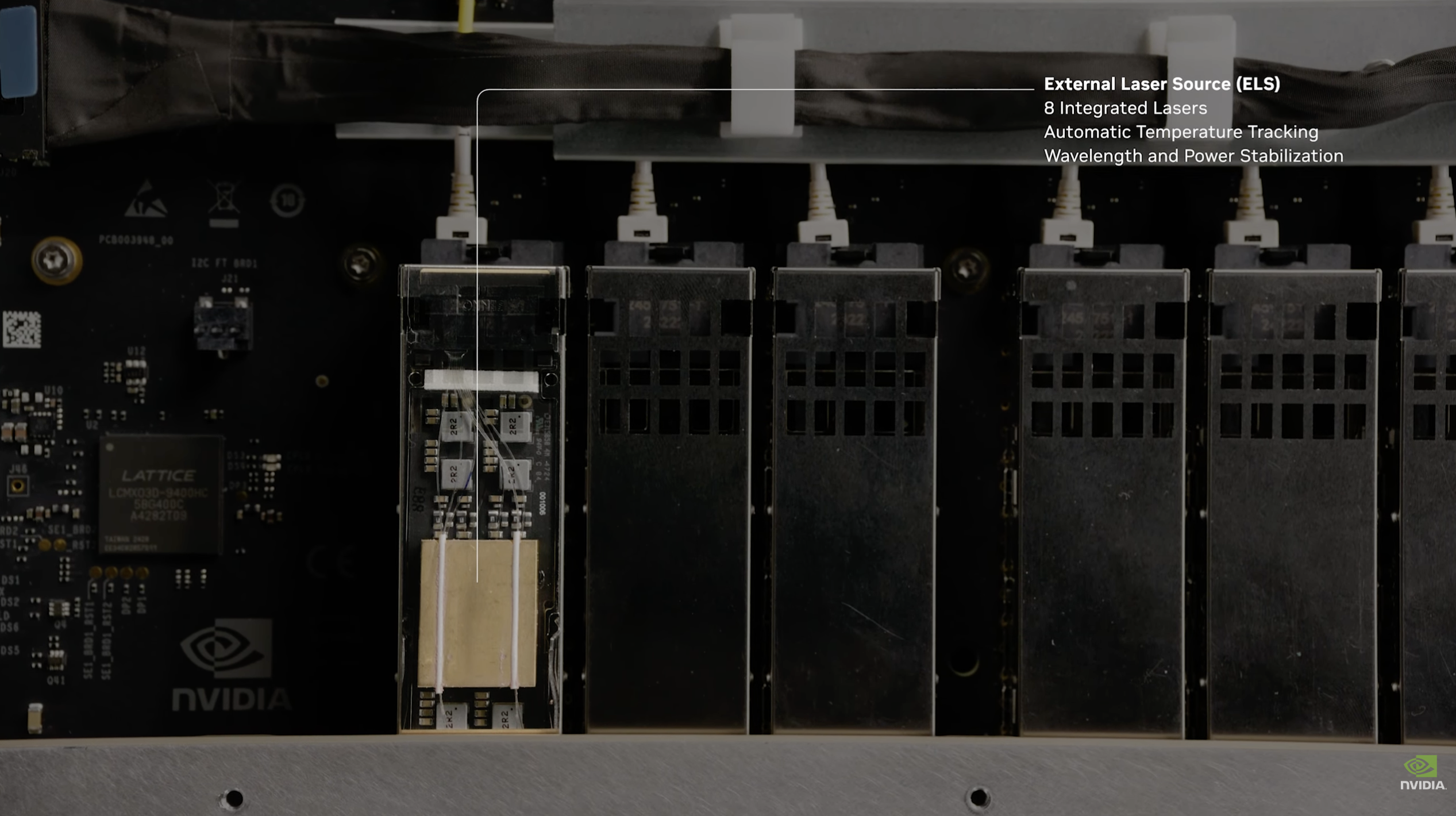
One ELS module. 8 integrated lasers per module · 18 modules per switch = 144 lasers total. Automatic temperature tracking and wavelength/power stabilization handled module-side, not in the SPE.
10) Inside — Multiplane Data Optical Connectors
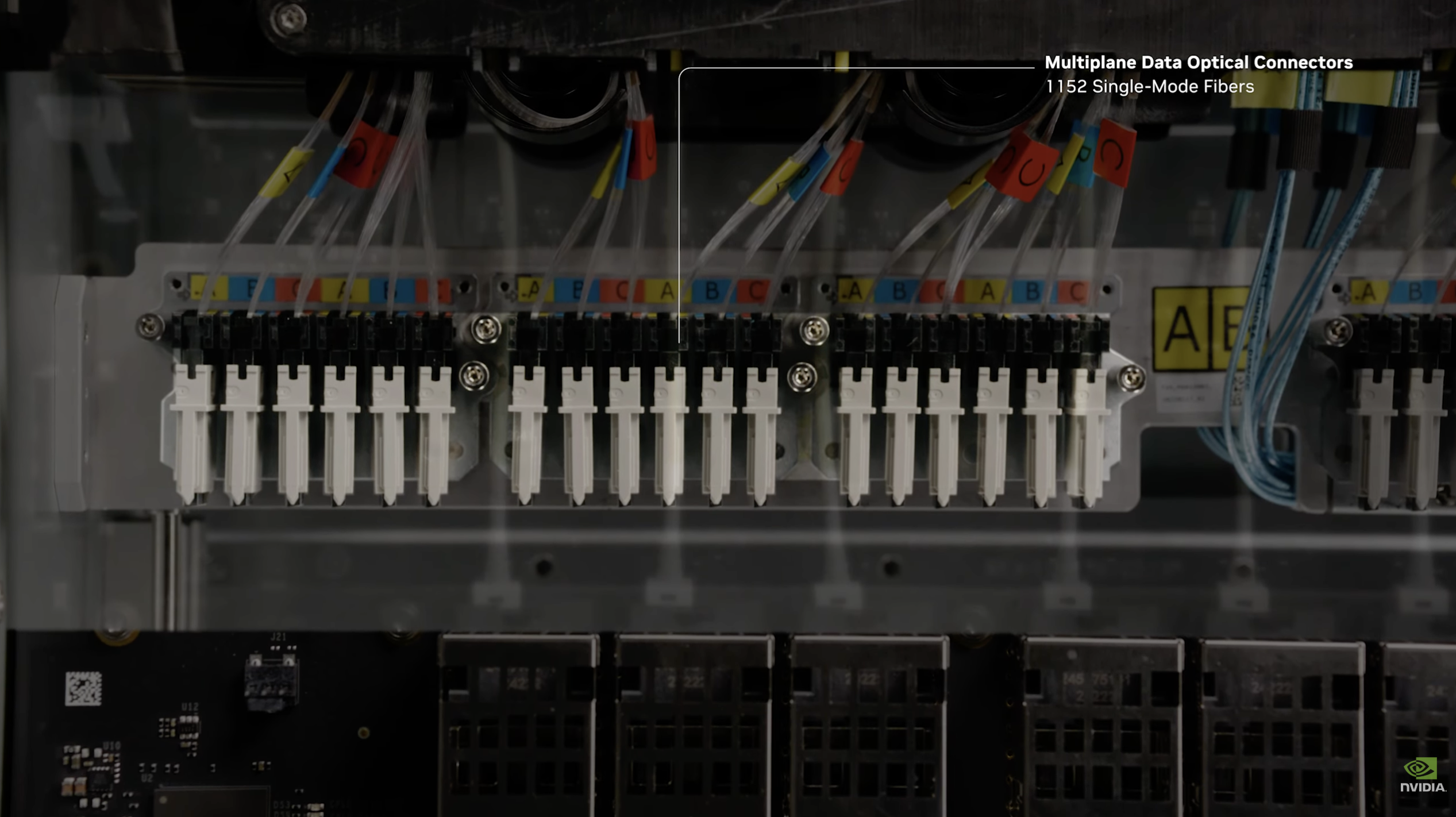
MMC-12 connector row. 1152 SMFs total = 144 ports × 8 fibers per port. High-density 12-fiber blocks replace the OSFP cages used in pluggable designs.
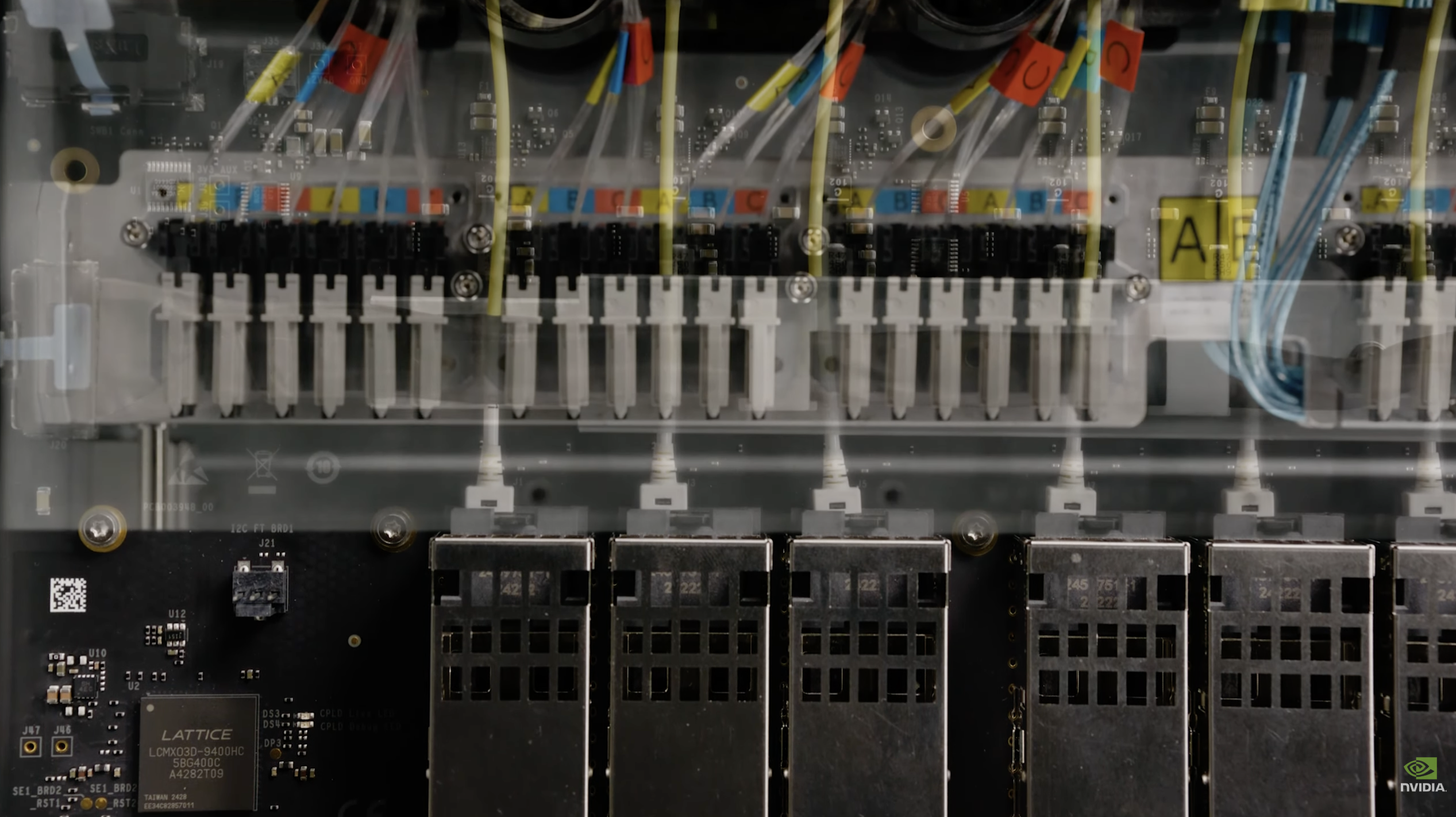
MMC connector array (top) meets front-panel cages (bottom). This is where light leaves the chassis and meets external MPO fiber cables.
11) Outside — front-panel, deployed
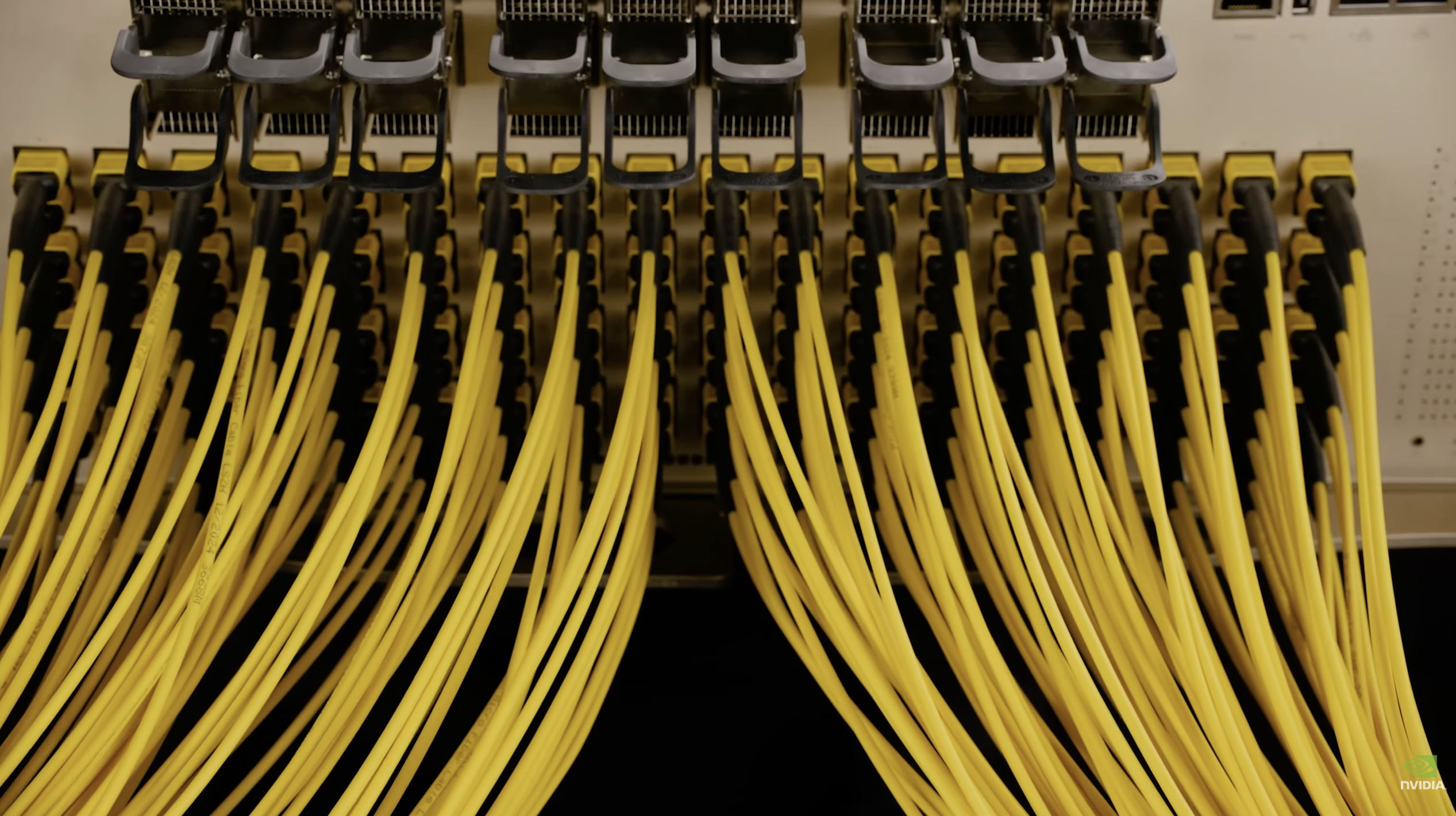
Closing shot. MPO fiber cables populated across all front-panel ports. From here, fibers run out to the GPU racks shown in image (1).
Quantum-X tends to be the choice for neoclouds and HPC-leaning operators; the InfiniBand discussion that follows assumes that audience.
Two switch variants — Q3400 (pluggable) and Q3450 (CPO)
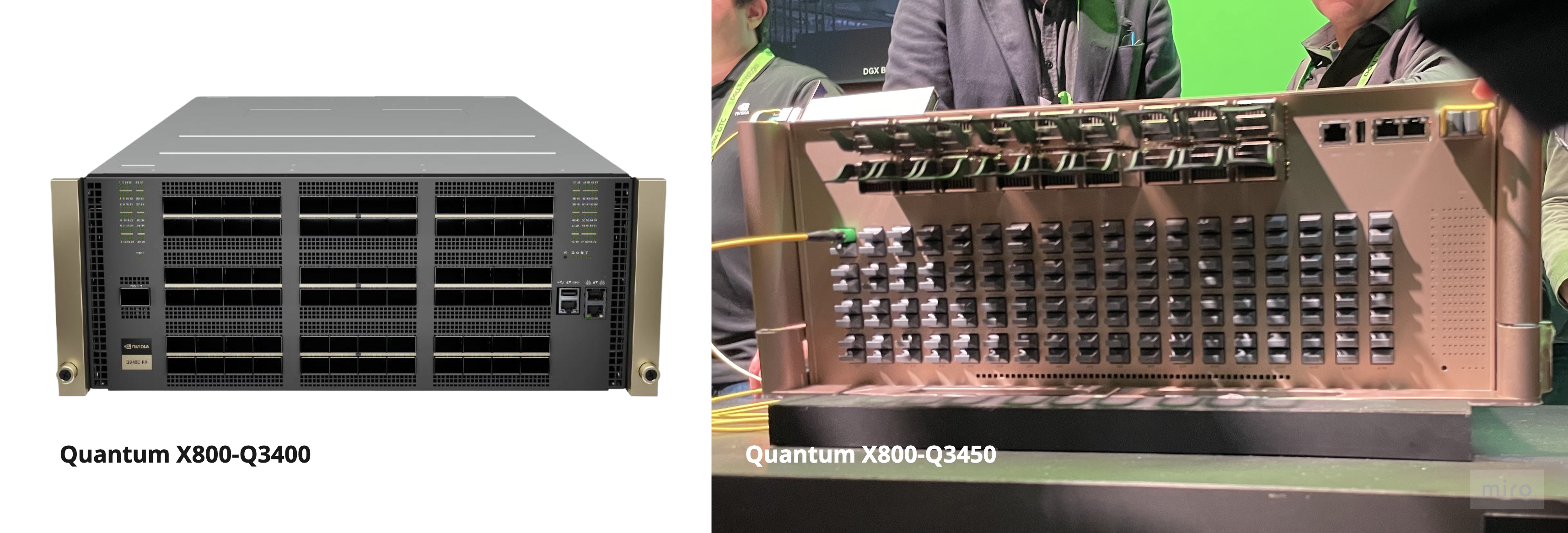
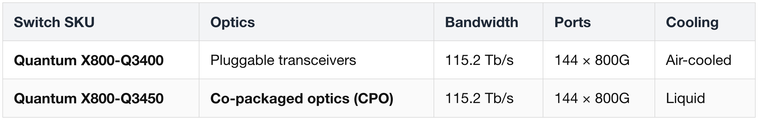
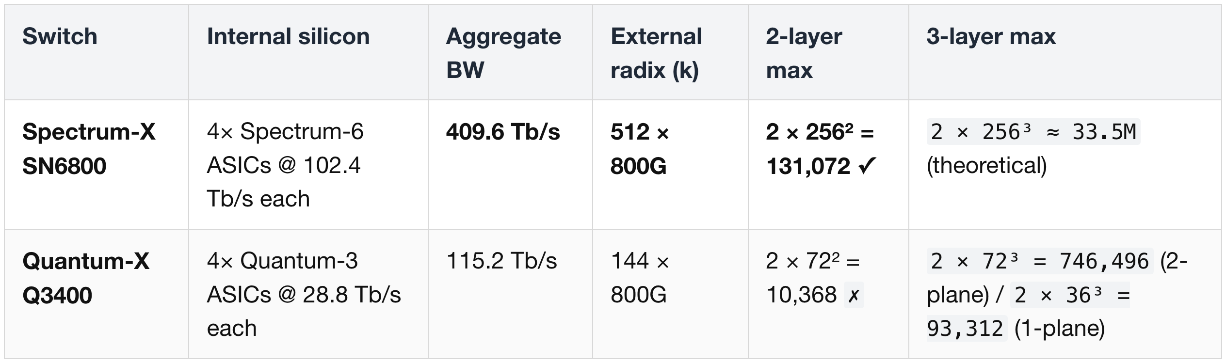
- Both expose 144 ports of 800G to the outside world, but internally each box contains 4× Quantum-3 ASICs (28.8 Tb/s each, summed to 115.2 Tb/s).
- When a NIC at the leaf layer connects to the switch box, its 800G signal is split four ways — 200G to each internal ASIC. From a topology standpoint, this is logically a 4-plane abstraction inside the box, but the box exposes it as a single switch to network engineers.
Multi-plane cluster scaling math
Cluster size scales with switch radix (k; the count of external ports a switch box exposes) and layers (L; tier of switches): Max GPUs = 2 × (k/2)^L
The three standard layer names
- Leaf — closest to the endpoints (the NICs on GPUs). Every NIC connects to a Leaf switch first. Sometimes called the "top-of-rack" or "ToR" layer.
- Spine — aggregation tier above the Leafs. Every Leaf connects to every Spine. Spine ↔ Spine traffic doesn't exist.
- Core (or "super-spine") — added only in 3-layer designs. Sits above the Spines and connects multiple Spine clusters together when one Spine layer's radix isn't big enough for the target cluster size.
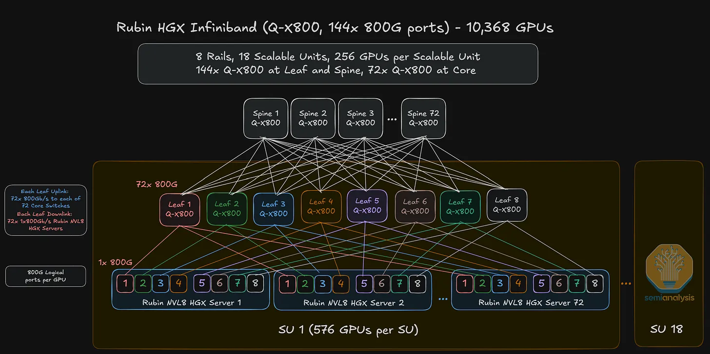
Two deployment options for VR NVL72:
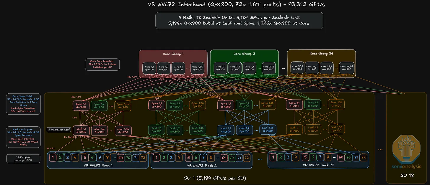
→ Sample calculation for 1-plane, 3-layer with 1,6T logical port deployment
- k=72 (number of logical 1.6Y ports per Q-X800 switch box),
- L=3 (Leaf, Spine, Core⎯three switch layers)
- plane count=1 ⇒ Max GPUs = 2 x 36³ = 93,312
1.6T logical port (single-plane network):
- the GPU's two 800G ports both connect to one leaf switch, presenting one 1.6T logical port per GPU.
- With Q3400's 115.2 Tb/s ÷ 1.6 Tb/s per logical port = effectively k = 72 logical 1.6T ports per box.
- Max cluster: 2 × (72/2)³ = 2 × 36³ = 93,312 GPUs at 3 layers.
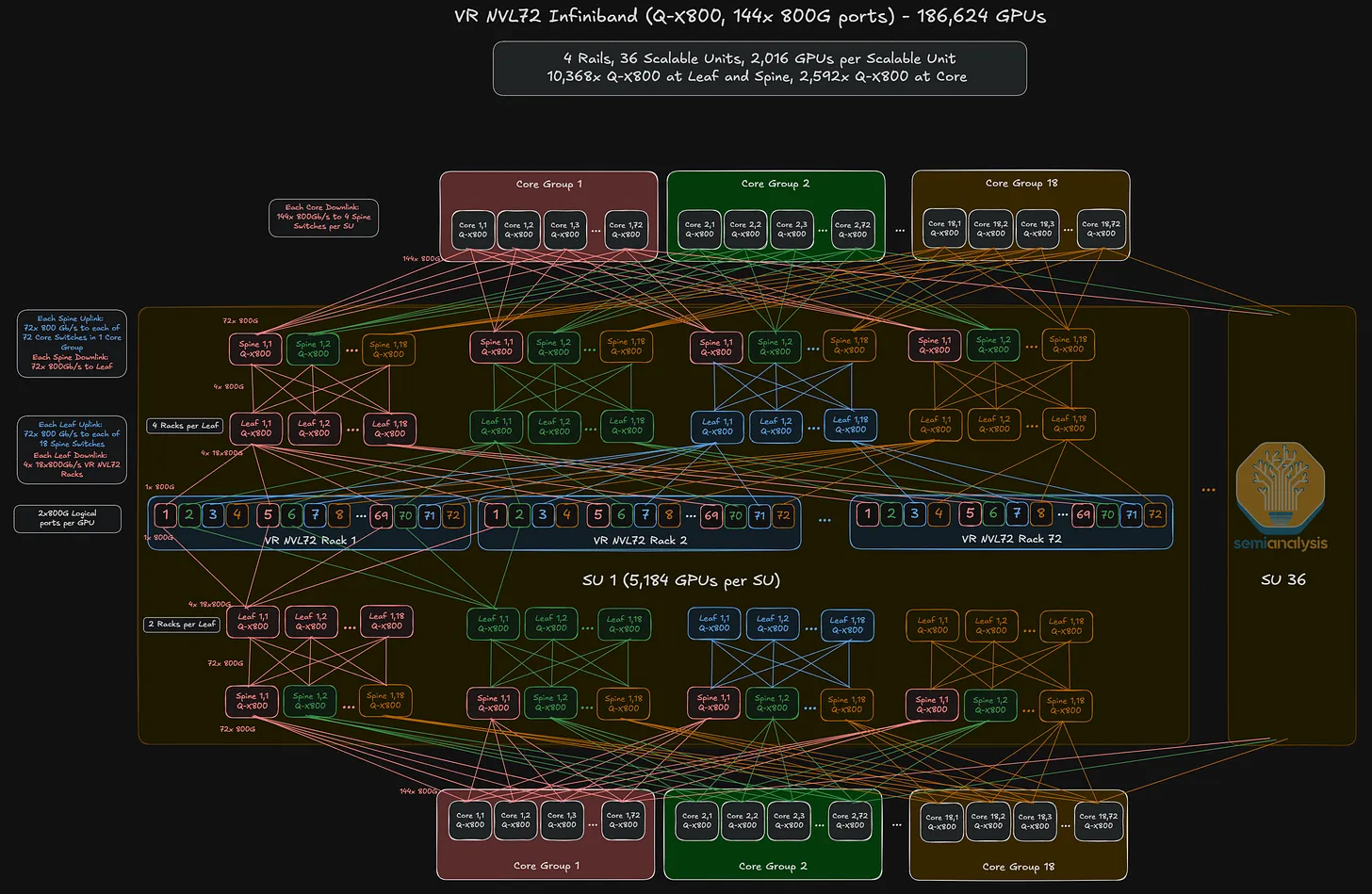
→ Sample calculation for k=144, L=3, plane count=2; not maxed-out, but reasonably scaled with 186,624 GPUs. Practical scale-out capacity has limitations due to a ceiling on infrastructure (floor space, power, cooling, optical cabling).
- Microsoft's Fairwater 2 in Atlanta, having the second highest current capacity after the Anthropic-Amazon New Carlisle datacenter (no.1 from the pure Grace-Blackwell series online perspective), is estimated to have ~300K GB200 GPUs online.
- Still doesn't reach the max cluster count when summed up.
2× 800G logical ports (2-plane network):
- each GPU's two 800G ports go to two different leaf switches on different planes.
- The full k = 144 × 800G port count is now in play per plane.
- Max cluster: 2 × (144/2)³ = 2 × 72³ = 746,496 GPUs at 3 layers.
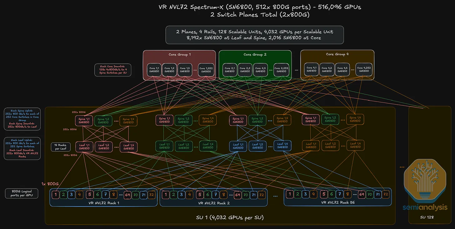
The 2-plane architecture is the expected reference deployment for VR NVL72 InfiniBand.
Note: the Q3400 / Q3450 exposes 144 external 800G ports per switch box.
At 2 layers of switching, that caps the cluster at2 × 72² = 10,368 GPUs— so any 100K-class InfiniBand cluster requires a 3-layer fabric (Leaf + Spine + Core).
The Ethernet equivalent — Spectrum-X SN6800, 512 external ports — can reach the same 100K+ in just 2 layers (see § 13). The protocol choice and the switch radix advantage are independent decisions, but the radix difference is what drives the layer-count gap.
NVL72 Front-Panel OSFP Cage Configuration
Each NVL72 compute tray has 8× 800G CX-9 NICs. Front-panel cage layout has two possibilities (this affects which scale-out topology — 1-plane or 2-plane — is physically wireable):
- Option A: 1× 1.6T OSFP cage per GPU → 4 cages per tray
- Option B: 2× 800G OSFP cages per GPU → 8 cages per tray⎯more popular; assumed base case for the scale-out architectures discussed in this section and § 13
Who Deploys InfiniBand
- More popular with neoclouds (CoreWeave, Lambda, others) than with hyperscalers.
- Reason: InfiniBand offers superior tail-latency control and lossless behavior, which matters for training workloads with strict synchronization requirements. Neoclouds optimize for raw training performance and tolerate the smaller supplier ecosystem (effectively Nvidia-only).
- Hyperscalers tend to prefer Ethernet because the open ecosystem allows in-house switch designs.
(13) Scale-Out — Ethernet Networks (Spectrum-X + Non-Nvidia)
This is the Ethernet counterpart to § 12 — same scale-out role, different protocol. Ethernet is the hyperscaler default for scale-out, and Nvidia's offering here is the Spectrum-X platform (the Ethernet sibling of Quantum-X covered in § 12).
There are two sub-flavors of Ethernet scale-out in practice: Nvidia's Spectrum-X family, and non-Nvidia silicon from Broadcom, Cisco, and Marvell.
Nvidia Spectrum-X — Three Switch SKUs (SN6000-LD Series)
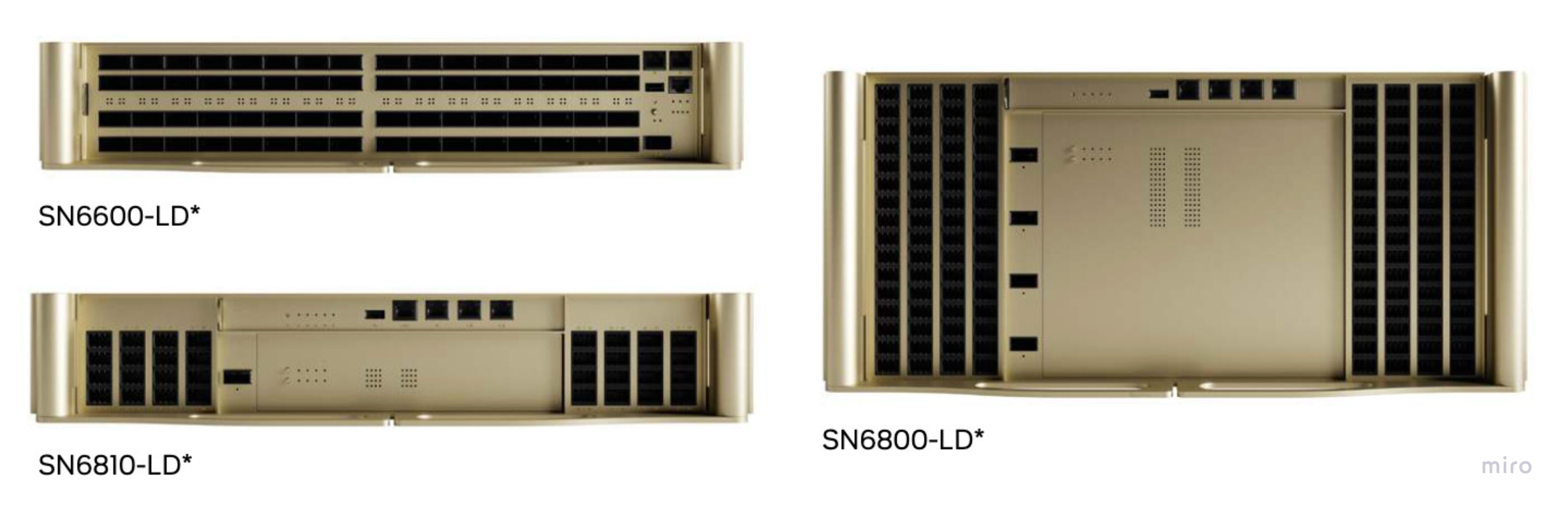
The shipping SN6000 family is the SN6000-LD generation — all three SKUs are liquid-cooled (LD = "Liquid-DC") and built on the Spectrum-6 ASIC. Model differentiation at a glance:
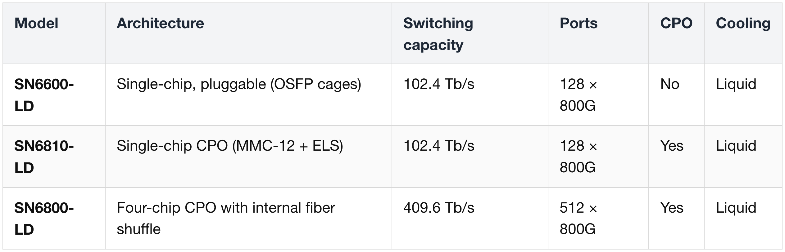
Key differentiators:
- Pluggable vs CPO split — SN6600-LD uses traditional OSFP cages with the existing pluggable transceiver ecosystem (integrated lasers); SN6800-LD and SN6810-LD use MMC-12 connectors (12-fiber high-density) with external laser source (ELS) modules routed into the switch package.
- SN6800-LD is the only 4-ASIC, 5RU (Rack Units) SKU — effectively four switches integrated into one box with an internal fiber shuffle.
- Same SerDes physics across all three — 8× 200G PAM4 per port — the differentiator is ASIC count and optical interface (CPO vs pluggable).
Both cross-rack compatibilities hold across all three SKUs:
- Power — 48/54 VDC busbar (40–60 V tolerance) is compatible with the GPU rack's 50 V busbar (§ 8).
- Cooling — 17–45 °C coolant inlet matches the rack warm-water envelope (Vera Rubin Decoded — Part 4 § 6); UQD8 v2 is the same QD standard used elsewhere in the rack.
Full per-SKU spec table (CPU, memory, packet buffer, ELS module count, dimensions, flow rates, etc., sourced from Nvidia's SN6000 datasheet) lives in Vera Rubin Decoded — Part 6 § 8 (Spectrum-X — Ethernet Scale-Out → Spectrum-X SN6000-LD Full Spec Table).
For the SN6600-LD (the most common pluggable Spectrum-X switch), the reference scale-out architecture is an 8-plane network: each GPU's 1.6 Tb/s scale-out bandwidth fans out 8 ways to 8 different leaf switches on 8 independent planes. Same 8-plane pattern applies to the SN6810-LD for CPO deployments.
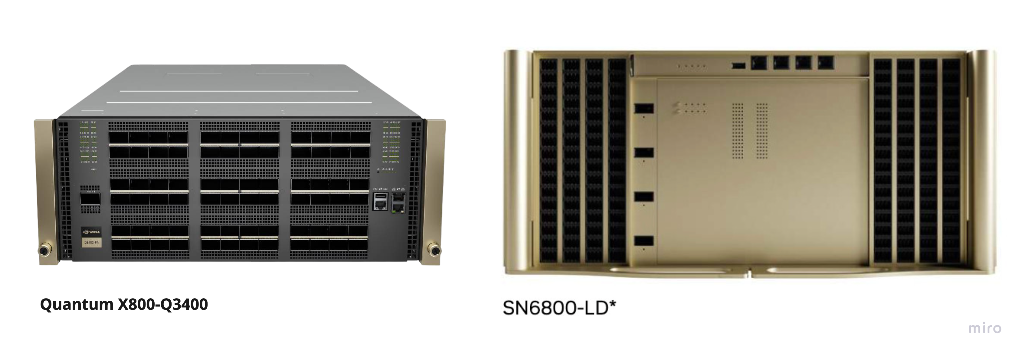
The SN6800 is the showcase CPO design:
- Each switch box contains 4× internal switch ASICs, similar to Quantum X800-Q3400's internal multi-plane abstraction.
- Each 3.2 Tb/s optical engine inside the box splits into 4 × 800G logical ports, all fan-out internally before exiting the front panel.
- An integrated fiber shuffle routes the 4 internal ASICs to the front-panel ports — eliminating external "octopus" cables and patch panels that pluggable-optics multi-plane deployments otherwise require.
- This is a critical operational simplification for multi-plane architectures at scale.
Cluster Scaling with High-Radix Switches
SN6600 Switch (pluggable)
→ via SN6600 — 512 × 800G ports
SN6810 switch (CPO)
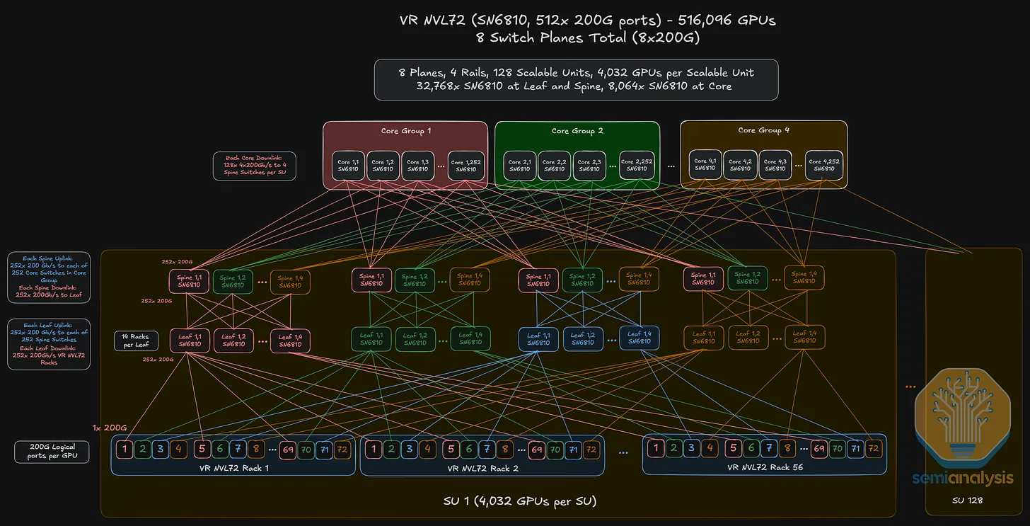
→ via SN6810 — 512 × 200G ports; sample calculation for k=512, L=3; not maxed-out
With a 512-port switch (SN6800 in 512 × 800G mode):
- 2-layer topology:
2 × (512/2)² = 2 × 256² = 131,072 GPUs - 3-layer topology:
2 × (512/2)³ = 2 × 256³ = 33,554,432 GPUs(theoretical ceiling — far beyond practical deployments)
Why Spectrum-X SN6800 Reaches 100K+ in Just 2 Layers (and Quantum-X Q3400 Doesn't)
The advantage of SN6800 over Quantum-X Q3400 for large-cluster deployments is switch radix, not the protocol. Both platforms use 4× internal ASICs per box, but each ASIC's bandwidth is very different — and that compounds at scale.
Reading the table:
- SN6800 reaches 100K+ GPUs in 2 layers (131,072 max) because its 512-port radix is large enough that
2 × (512/2)² ≥ 100,000. - Q3400 only reaches 10,368 GPUs in 2 layers — to exceed 100K, it needs a 3rd switching layer.
- The root cause is per-ASIC bandwidth: each Spectrum-6 ASIC moves ~3.5× more data than each Quantum-3 ASIC (102.4 Tb/s vs 28.8 Tb/s), translating directly into 3.5× more 800G external ports per box at the same 4-ASIC internal structure.
Practical implication
- 100K-class Ethernet clusters: 2-layer SN6800 fabric is sufficient.
- 100K-class InfiniBand clusters: must use a 3-layer Q3400 / Q3450 fabric (plus the additional optical + fiber + transceiver cost of that 3rd layer).
- This is part of why hyperscalers leaning toward Ethernet (Spectrum-X or non-Nvidia) get a meaningful cost / operational simplicity advantage at very large cluster sizes.
Why CPO matters (and where it doesn't)
Power
Power savings: an 800G DR4 pluggable transceiver burns 16–17 W. Equivalent CPO optical engines + external laser source modules use ~70% less power for the same 800G. Translates to ~10% reduction in total networking-equipment power in a 3-layer HGX Rubin NVL8 cluster — though only ~1% of total cluster power (since GPU power dominates).
Per-rack power demand basis for a GB300 NVL72 (sample calculation):
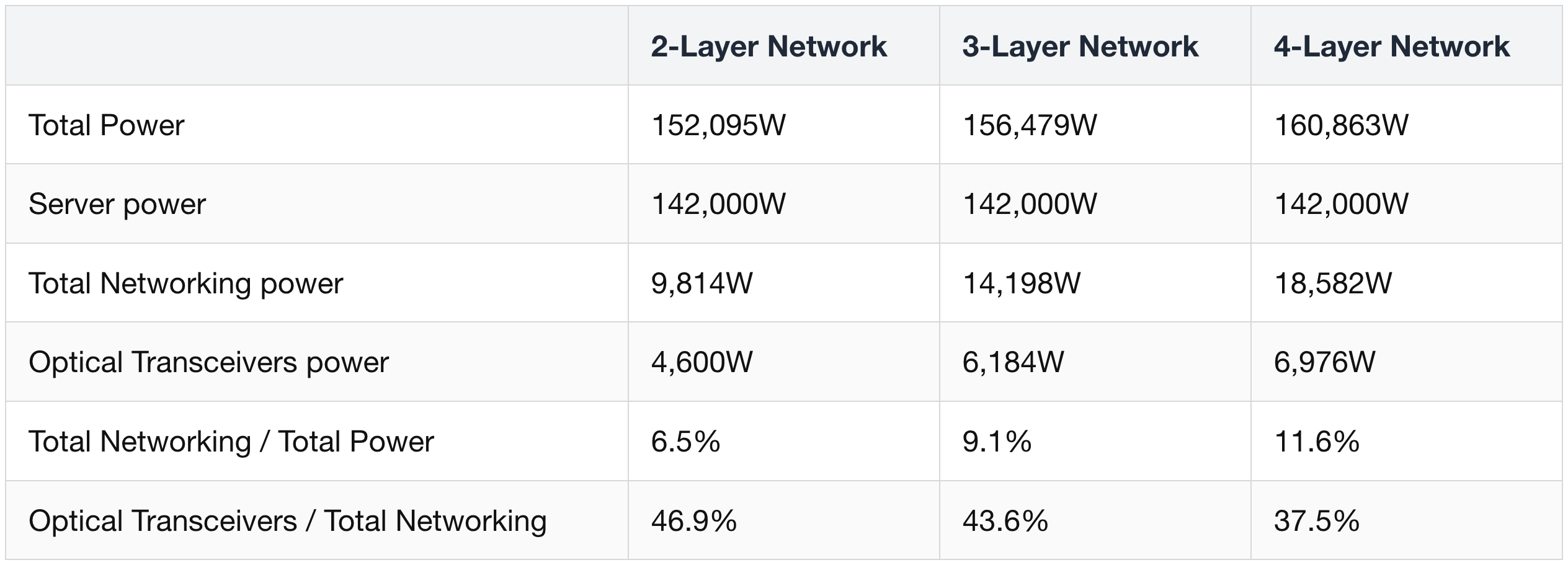
Optical transceivers alone consume close to 50% of total networking power.
This is why the shift from pluggable transceivers to CPO is happening:
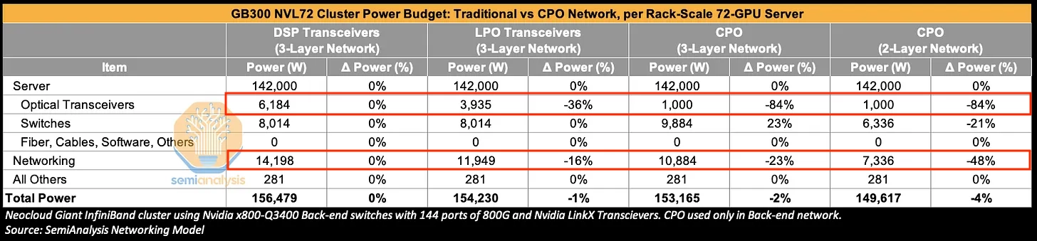
On a 3-layer GB300 NVL72 cluster, swapping DSP transceivers for CPO cuts transceiver power by 84% and networking power by 23%.
However, at the cluster level, the effect gets diluted:
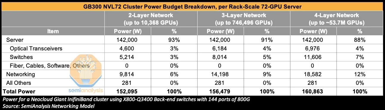
- Networking power is only ~9% of total cluster power.
- So a transceiver power -84% / networking power -23% reduction translates to roughly a 2% saving on total cluster power.
- A 2-layer CPO network can produce a larger networking-power reduction, but total cluster power saving still tops out at roughly 4%.
Cost
Cost savings: ~75% reduction in transceiver costs vs Nvidia's LinkX pluggable optics (Nvidia's optics are priced at a significant premium). Again material at the networking-cost level, less so at the full-cluster level.
Per-rack cost basis for a GB300 NVL72:
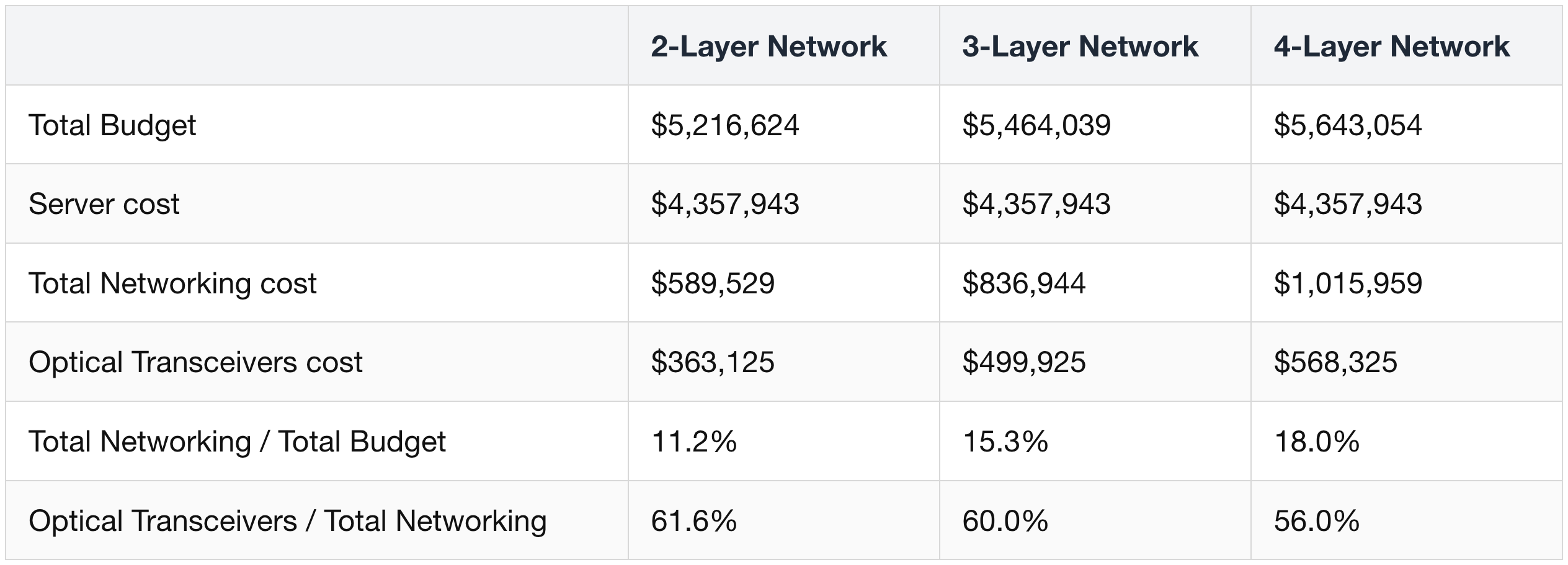
The same dilution shows up on the cost side:
- On a 3-layer network, total networking cost can fall ~21% with CPO, but total cluster cost only drops ~3%.
- On a 2-layer CPO network, total networking cost can fall ~46%, but total cluster cost saving tops out at ~7%.
Reliability: transceiver link flaps are a real operational headache at scale. Meta presented results at ECOC 2025 showing strong CPO reliability across 15M port-device hours of testing — equivalent to about 15 CPO switches running for 11 months. Encouraging, but still early.
Simplified multi-plane deployment: the SN6800's integrated fiber shuffle is the operational win that justifies CPO adoption for multi-plane architectures. Without it (pure pluggable), each GPU's fan-out across multiple planes requires external fiber shuffle boxes + patch panels + complex octopus cables — all of which become operational liabilities at scale.
Who's adopting CPO: primarily neoclouds (CoreWeave, Lambda) where deployment simplicity directly pays off. Hyperscalers move slower because their fleets are large and CPO-vendor switching has higher implementation cost.
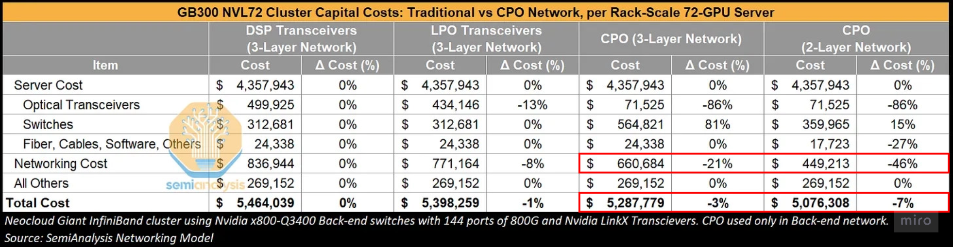
Non-Nvidia Ethernet — the hyperscaler reality
Most hyperscalers don't run Nvidia-branded switches in the scale-out fabric. They use third-party silicon:
- Broadcom Tomahawk 6 — 102.4 Tb/s ASIC, with a Tomahawk 6 CPO variant in development. The dominant choice for hyperscalers.
- Cisco Silicon One G300 — recently announced 102.4 Tb/s ASIC.
- Marvell Teralynx — alternative ASIC line, less common in this generation.
Two main deployment topologies with these:
- 8-plane "flat" network — uses the switch's full 512-radix capacity, each GPU fanning across 8 planes.
- Single-plane network with 1.6T OSFP cages at the NIC — simpler topology, used when fan-out flexibility matters less.
Meta and xAI — specific deployment notes
- Meta is building VR NVL72 clusters as NSF (Non-Scheduled Fabric) clusters using Broadcom Tomahawk 6-based Minipack-4 switches (102.4 Tb/s, OCP rack-scale form factor). Optics for switch-to-switch links, 1.6T AECs (Active Electrical Cables) for NIC-to-TOR.
- The gearbox catch: If Minipack-4 isn't ready when Meta needs to deploy, they fall back to 51.2T Minipack-3 switches. Minipack-3 has 100G-per-lane SerDes; the CX-9 NIC has 200G-per-lane SerDes. So gearboxes have to be embedded inside the AECs to bridge 200G ↔ 100G. Credo Semiconductor makes those AECs and gains pricing power as a result.
- 1.6T AECs ramp in H2 2026.
- xAI is expected to use 1.6T AECs everywhere — NIC-to-TOR, switch-to-switch, leaf-to-spine, spine-to-core — in a single-plane network. This eliminates most transceiver content at the switch boxes (which would otherwise be huge cost centers).
- For both, Credo Semiconductor is the AEC vendor benefiting most.
Net deployment picture for a typical hyperscaler
- Inside the rack: NVLink 6 (no alternative)
- Scale-out: Broadcom Tomahawk 6 (or Cisco G300) — not Nvidia Spectrum-6
- Short reach (NIC ↔ TOR): 1.6T AECs (Credo)
- Long reach (switch ↔ switch): pluggable optical transceivers (CPO adoption rare in the first 1–2 years)
- DPU slot: in-house DPU or bare CX-9 NIC, not BlueField-4 (see next section)
This is where Nvidia's "extreme co-design" thesis runs into hyperscaler economics. The scale-up domain belongs to Nvidia. The scale-out domain belongs to whoever can ship custom silicon faster and cheaper.
(14) Customization — What Hyperscalers Actually Swap
Nvidia allows customization on only three modules, and the rest must follow the reference design:
- BlueField-4 Module — most hyperscalers swap for their in-house DPU or a bare CX-9 (cheaper)
- Power Delivery Module — hyperscalers often substitute their own design (especially for HVDC deployments)
- System Management Module — hyperscalers usually ship their own SMM/TPM/DC-SCM combination
All other modules (Strata, Orchid, Midplane) must follow Nvidia's reference design and form factor. Any substitution still has to physically mate with the midplane's Paladin HD2 connector pattern.
(15) Summary — How the Six (Now Seven) Chips Become One Rack
The full story in one page: seven silicon products (six original + Groq 3 LPX) assemble into modules, modules into a compute tray, trays into a rack, and racks into a cluster. Each layer has its own engineering decisions and its own supplier ecosystem — and each is documented in a specific part of this six-part series.
1) The Connection Hierarchy at a Glance
Reading the layered view: a chip in one rack reaches another chip in the same rack via Midplane PCIe Gen6 + NVLink 6 copper backplane. A chip in a different rack adds CX-9 + optical Ethernet/InfiniBand on top of that. Everything above the rack boundary is optics.
2) What Got Engineered Differently This Generation
The non-obvious changes — the ones that took real silicon, PCB, mechanical, and supply-chain work:
Inside the tray (Part 4)
- Cableless midplane design (Part 4 § 4) — Paladin HD2 board-to-board connectors replace the GB200/GB300 flyover cables that caused most assembly failures. Result: 1.5h → ~5min tray assembly (18× faster).
- PCB material upgrade (Part 4 § 5) — M7/M8 → M8+/M9 CCL (Panasonic Megtron standard), HVLP2 → HVLP4 copper foil, optional Quartz cloth on Orchid + Midplane. PCB area grows ~2.3× vs GB300, directly tied to the cableless design forcing PCIe Gen6 to traverse 500 mm of trace.
- 100% liquid cooling (Part 4 § 6) — no fans in the tray. Coolant enters via UQDs, distributes via internal manifold to MQDs on each module's cold plate.
Rack-level cooling (Part 4)
- 45 °C warm-water cooling (Part 4 § 7) — operating envelope extended to 45 °C inlet, opening the door to chiller-less deployments (already pioneered by Firmus on GB200). Outlet ceiling ~65 °C; 2–2.5× higher flow required to compensate for tighter delta-T.
- Dual-loop facility architecture (Schneider RD111 reference) — warm liquid loop for cold plates + chilled water for residual air cooling.
Power delivery (this part)
- 50 V busbar at 5,000 A+ (§ 8) — liquid-cooled, ~2× the current of GB200. Drives the I²R-minimized chain: AC mains → 50 V → 12 V on Strata's IBC → ~1 V at the chip.
- HVDC option (§ 9) — separate power rack at 800 VDC (Nvidia spec) or ±400 VDC (OCP spec), feeding 50 V step-down shelves inside the GPU rack. Plus Meta's "high-power rack" integrating BBU + CBU for peak shaving.
Networking
- Bidirectional NVLink 6 SerDes (covered in Part 3 § 5, NVLink 6 Switch) — same ~5,000 backplane cables as GB300, but each carries 2× the data via simultaneous bidirectional signaling.
- Quantum-X vs Spectrum-X (§ 12 vs § 13, this part) — Nvidia's two parallel scale-out networking platforms. Quantum-X = InfiniBand (neoclouds); Spectrum-X = Ethernet (hyperscalers). The "-X" means photonics-enabled on either family.
- Switch radix matters more than protocol — Spectrum-X SN6800's 512-port radix reaches 100K+ GPUs in 2 layers; Quantum-X Q3400's 144-port radix needs 3 layers for the same scale.
3) Form Factor — Two Deployable Options
Rubin ships in two parallel form factors corresponding to Nvidia's two design philosophies (Part 4 § 2):
- HGX Rubin NVL8 — server-scale chassis (8 GPUs), OEM-customizable. Lower scale-out BW per GPU (800 G), single-plane 8-rail topology.
- VR NVL72 — rack-scale (72 GPUs), Nvidia-defined (DGX-style). Higher scale-out BW per GPU (1.6 T via 2× CX-9), 1- or 2-plane topology.
Adoption pattern: neoclouds tend toward DGX (NVL72) for turnkey speed; hyperscalers tend toward HGX for fleet customization.
4) What's Standard vs Customizable
Out of the 6+ modules per compute tray, Nvidia allows hyperscaler customization on only three:
- BlueField-4 Module — most hyperscalers swap for in-house DPU or bare CX-9
- Power Delivery Module — substituted in HVDC deployments
- System Management Module (SMM / TPM / DC-SCM) — usually in-house designs
Everything else — Strata, Orchid, Midplane, NVLink backplane, NVLink switch trays — must follow Nvidia's reference design.
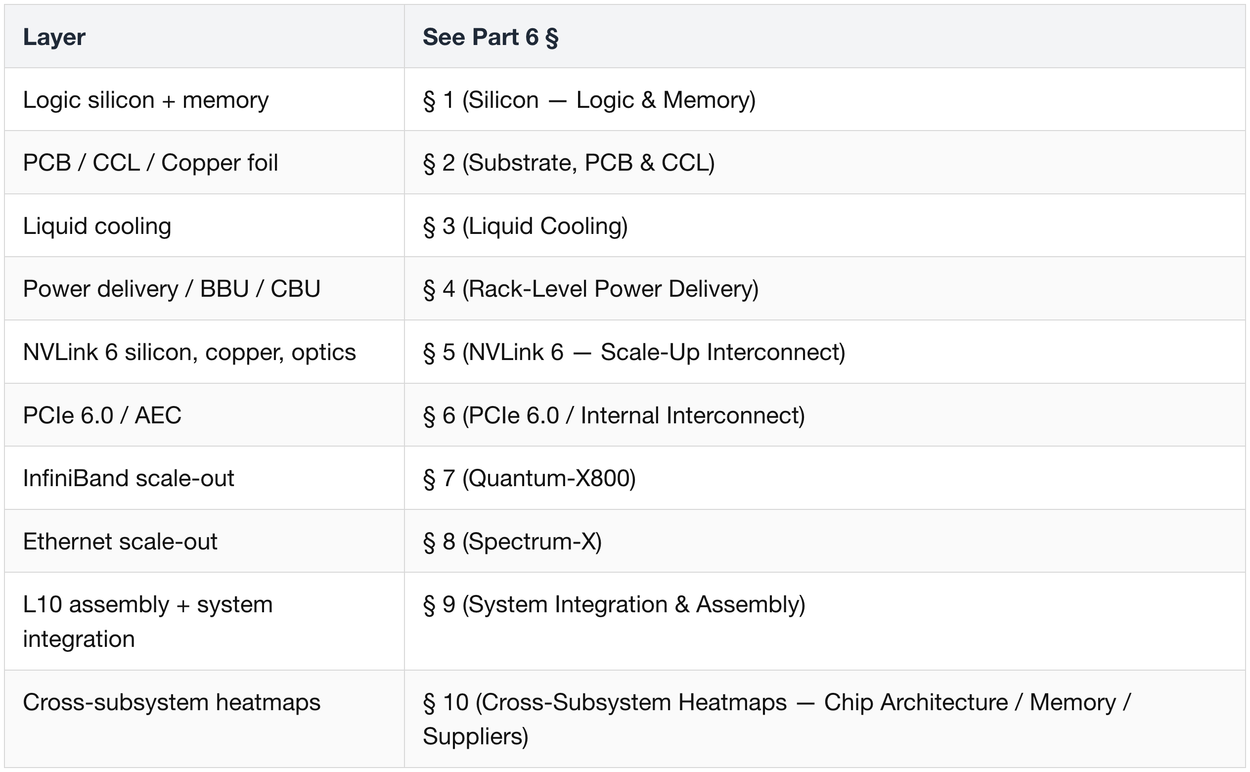
5) Supplier Landscape
The full multi-layer supplier landscape — by subsystem (silicon, memory, PCB/CCL, cooling, power, NVLink 6, PCIe 6, Quantum-X800, Spectrum-X, system integration), with commercial timelines, strategic partnerships, and a cross-subsystem heatmap — is consolidated in Part 6 (Supply Chain — Master Reference).
The supplier landscape was placed in its own part because it spans the entire chip-to-rack stack and reads better organized by subsystem than by the engineering narrative.
Layer-by-layer pointer for navigation within Part 6:
6) Where to Read What — Series Map
The full six-part Vera Rubin Decoded series:
| Part | Title | Scope |
|---|---|---|
| 1 | Platform Framing & Architecture Map | Blackwell → Rubin platform thesis, headline specs |
| 2 | Rubin GPU — Engineering Deep Dive | Process node, SMs, HBM4, NVLink-C2C, package, CPX + Groq 3 LPX |
| 3 | Vera CPU & the Networking Silicon Family | Vera CPU, NVLink 6 Switch, ConnectX-9, BlueField-4, Spectrum-6 |
| 4 | Rack Assembly — Trays, PCB, and Cooling | HGX vs NVL72, compute tray modules, cableless midplane, PCB upgrade, liquid cooling |
| 5 | Rack Power and the Networking Fabric (this part) | Power delivery, HVDC, tray↔rack wiring, scale-up NVLink 6, scale-out InfiniBand + Ethernet |
| 6 | Supply Chain — Master Reference | Suppliers by subsystem across the entire stack |
7) One-Line Read of the Whole Thing
- The chips (Parts 2–3) push every silicon spec to the edge of what suppliers can build.
- Part 4 § 2 reveals those chips can be deployed in two form factors — HGX server or VR NVL72 rack.
- Part 4 §§ 3–7 and this part (Part 5 §§ 8–14) walk through how the rack-scale form factor is mechanically assembled, electrically powered, thermally managed, and optically interconnected into a single 72-GPU accelerator that hyperscalers and neoclouds will buy and operate as the foundational unit of AI infrastructure for the next 2 years.
The two design decisions at the top — treat the rack as the unit of compute and push every component to the edge of supplier capability — drive every downstream engineering trade-off documented across the series.