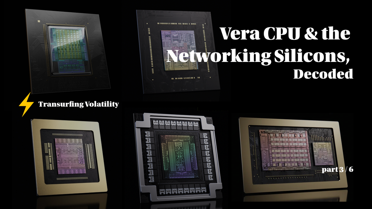
Vera Rubin Decoded Pt. 3 | Vera CPU & the Networking Silicon Family
Where to Read What — Series Map
| Part | Title | Scope |
|---|---|---|
| 1 | Platform Framing & Architecture Map | Blackwell → Rubin platform thesis, headline specs |
| 2 | Rubin GPU — Engineering Deep Dive | Process node, SMs, HBM4, NVLink-C2C, package, CPX + Groq 3 LPX |
| 3 | Vera CPU & the Networking Silicon Family (this part) | Vera CPU, NVLink 6 Switch, ConnectX-9, BlueField-4, Spectrum-6 |
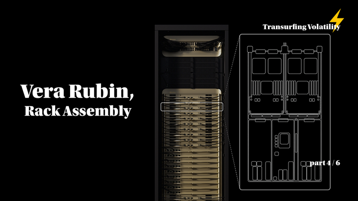
| 4 | Rack Assembly — Trays, PCB, and Cooling | HGX vs NVL72, compute tray modules, cableless midplane, PCB upgrade, liquid cooling |
| 5 | Rack Power and the Networking Fabric | Power delivery, HVDC, tray↔rack wiring, scale-up NVLink 6, scale-out InfiniBand + Ethernet |
| 6 | Supply Chain — Master Reference | Suppliers by subsystem across the entire stack |
4. Vera
Vera is Nvidia's second-generation in-house ARM-based CPU, succeeding Grace in the Blackwell platform. The design intent has shifted:
- Grace was a host CPU sitting alongside the GPU.
- Vera is positioned as a data engine — its job is to keep the Rubin GPU fed by moving data, orchestrating workloads, and handling control flow at a rate that matches the GPU's throughput.
At Rubin-class GPU speeds, a standard server CPU becomes the bottleneck. Vera is engineered specifically to remove that bottleneck.
Grace → Vera at a glance
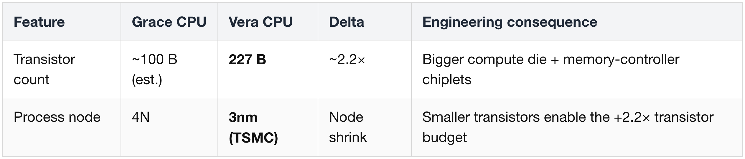
The changes group into four engineering layers: what executes, what stores/feeds it, what moves it in and out of the chip, and what silicon it all runs on. Each table below pairs the raw spec delta with the engineering consequence — this is the canonical reference for the rest of the Vera section.
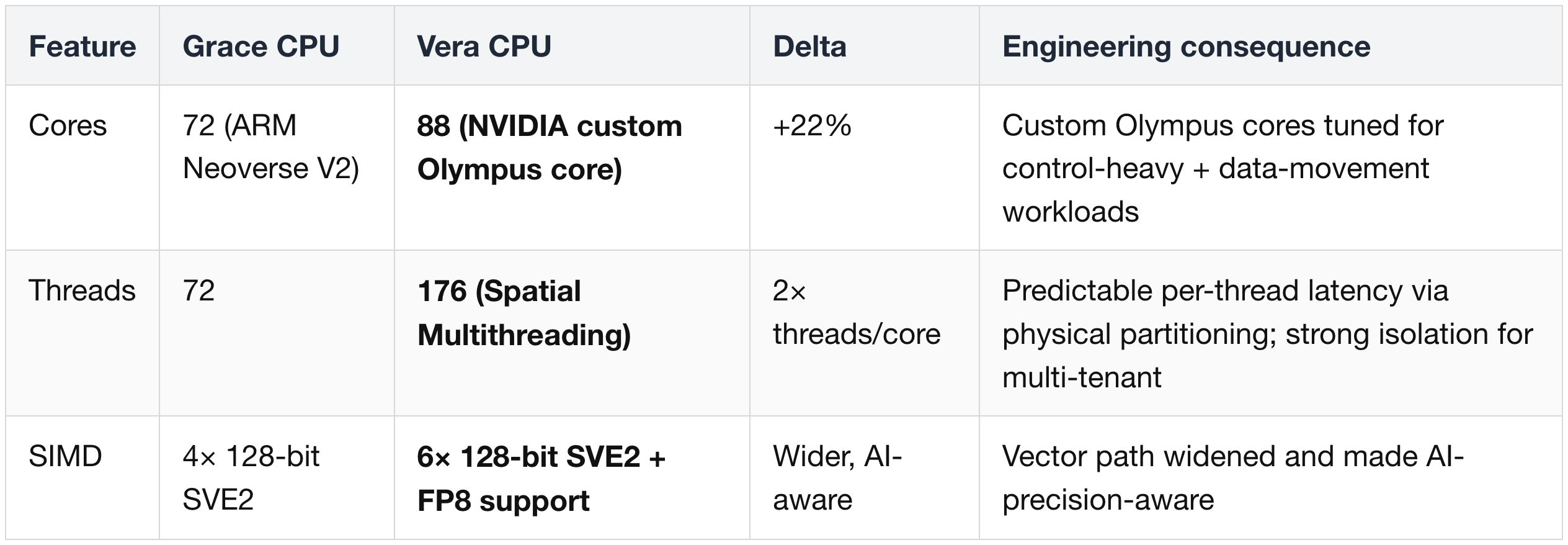
Compute (Cores · Threads · SIMD)
Cache & Memory Subsystem
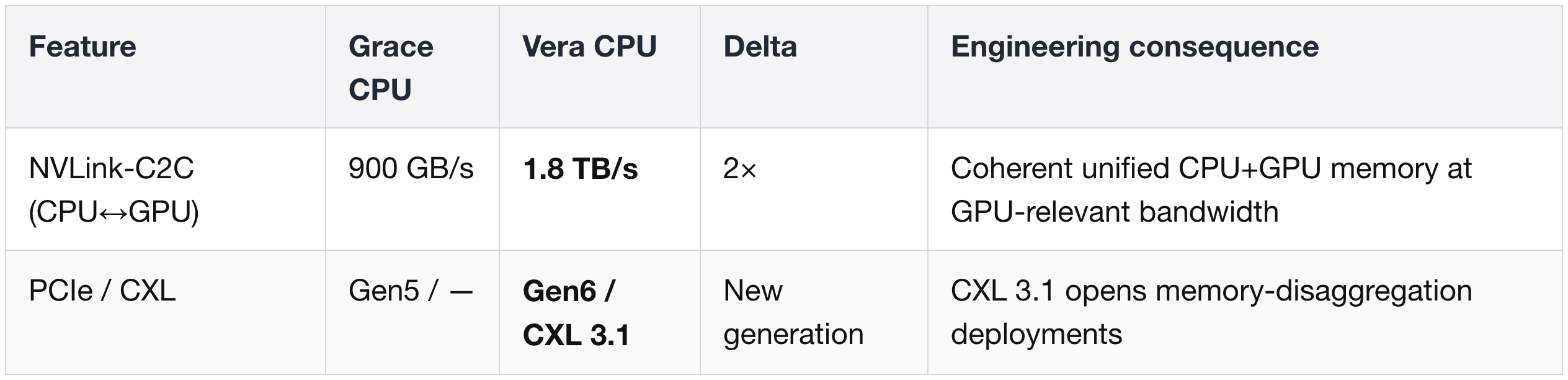
Interconnect & Standards
Silicon
(1) Olympus Cores & Spatial Multithreading
Vera moves away from ARM's off-the-shelf Neoverse V2 cores (used in Grace) to Nvidia's custom ARM-compatible "Olympus" cores — the return of Nvidia's own CPU core design.
- Olympus is a wide, deep microarchitecture with improved branch prediction, prefetching, and load-store performance.
- Specifically optimized for control-heavy and data-movement-intensive workloads (the actual bottleneck profile of feeding modern GPUs), not generic enterprise compute.
- Fully ARM v9.2 compatible — existing ARM Linux distros, frameworks, and orchestration software run unmodified.
What Spatial Multithreading is (and how it differs from SMT)
Traditional Simultaneous Multi-Threading (SMT — used by Intel as "Hyper-Threading" and by AMD on Zen cores) lets two threads share a single core by time-slicing the core's execution resources. This boosts throughput but introduces unpredictable per-thread latency and security side-channels.
- Vera's Spatial Multithreading runs two threads per core by physically partitioning resources instead of time-slicing them.
- Result: 176 hardware threads across 88 cores, with predictable per-thread latency and stronger isolation between threads.
- Critical for multi-tenant AI factories where one tenant's workload should not affect another's response time.
Die-level yield trick
- Nvidia actually prints 91 cores on the die but ships only 88 enabled.
- The 3 redundant cores exist purely to improve manufacturing yield — if any of the 91 cores has a defect, it gets disabled and the chip still ships as a full 88-core part.
- This is the same idea as floor-sweeping on the GPU side.
(2) Memory Subsystem — SOCAMM + LPDDR5X
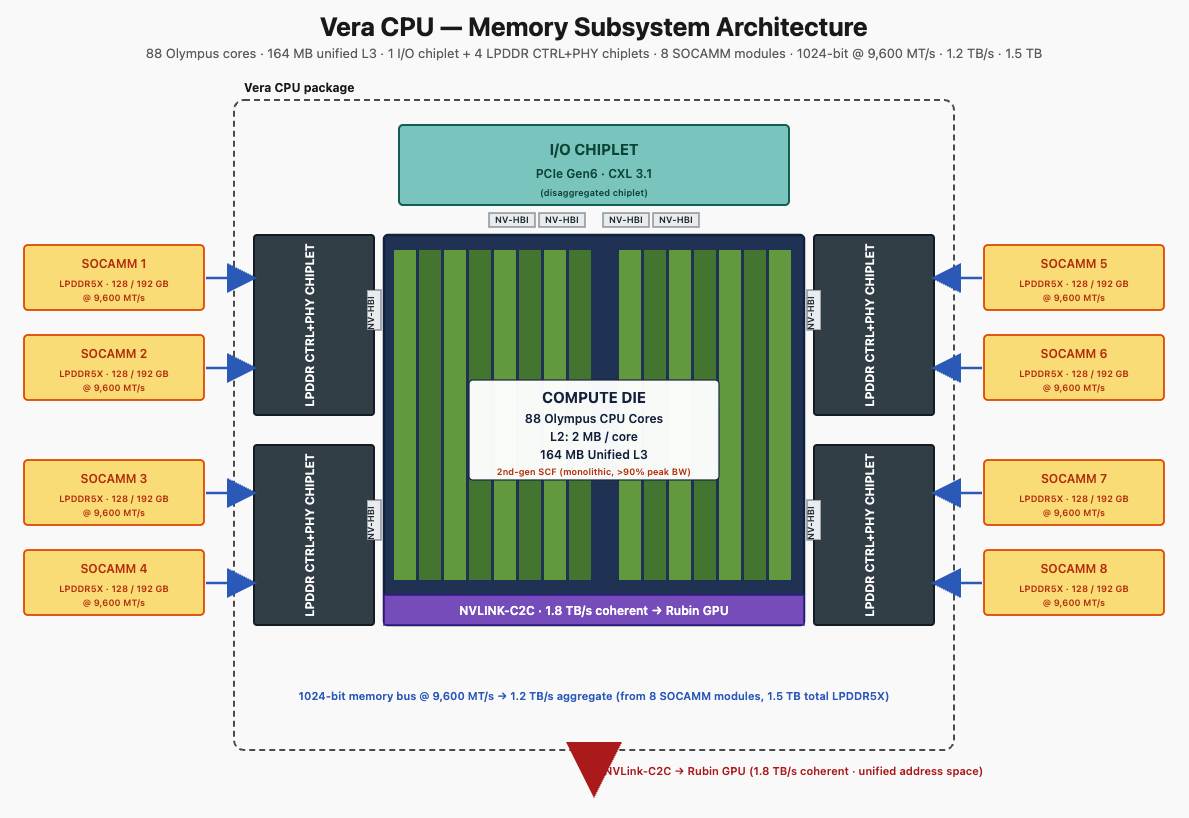
Vera's memory subsystem is rebuilt to triple capacity and 2.4× bandwidth versus Grace.
- LPDDR5X (Low-Power DDR5X) is the memory type used in modern smartphones and laptops — far more power-efficient per GB/s than standard server DDR5, at the cost of being soldered or modularly attached close to the CPU.
- Vera uses SOCAMM modules — Small Outline Compression Attached Memory Modules — Nvidia's serviceable LPDDR5X form factor, designed for data center reliability/replaceability requirements.
- 8 SOCAMM modules per Vera socket, totaling up to 1.5 TB at 9,600 MT/s.
- 1024-bit memory bus (double Grace's 512-bit) is what lets total bandwidth reach 1.2 TB/s while keeping clock speeds reasonable.
Why memory bandwidth matters this much
- At 22 TB/s of HBM bandwidth on the Rubin GPU side, the CPU side previously looked thin.
- Vera's 1.2 TB/s LPDDR5X is the second tier of the unified memory pool exposed to applications via NVLink-C2C (see Rubin section (4)).
- A KV cache that has overflowed Rubin's 288 GB HBM4 needs to land somewhere fast — Vera's LPDDR5X is that landing zone. If Vera's memory bandwidth were too low, the offload path would stall the GPU.
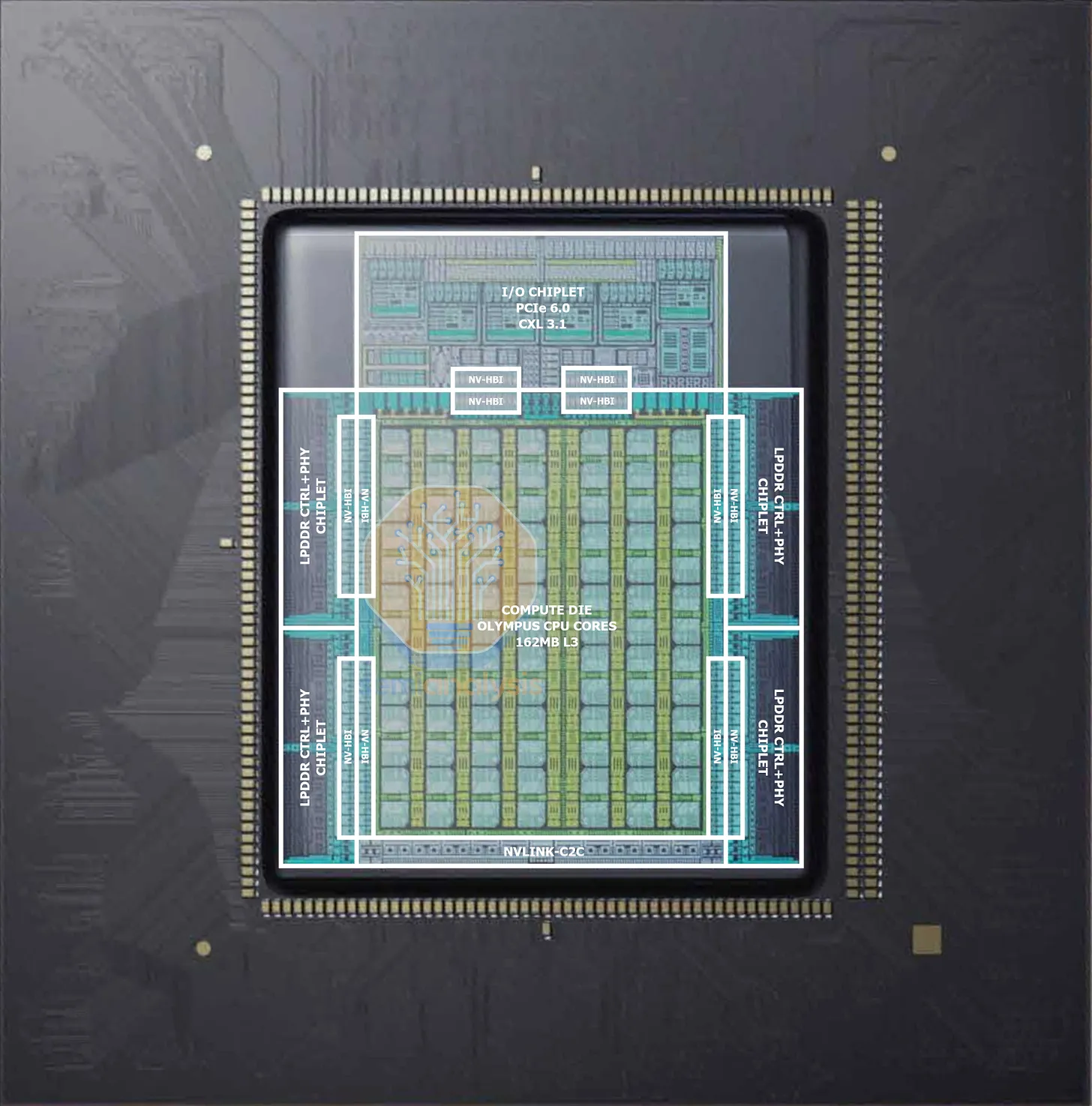
(3) Scalable Coherency Fabric (SCF) — On-die Data Movement
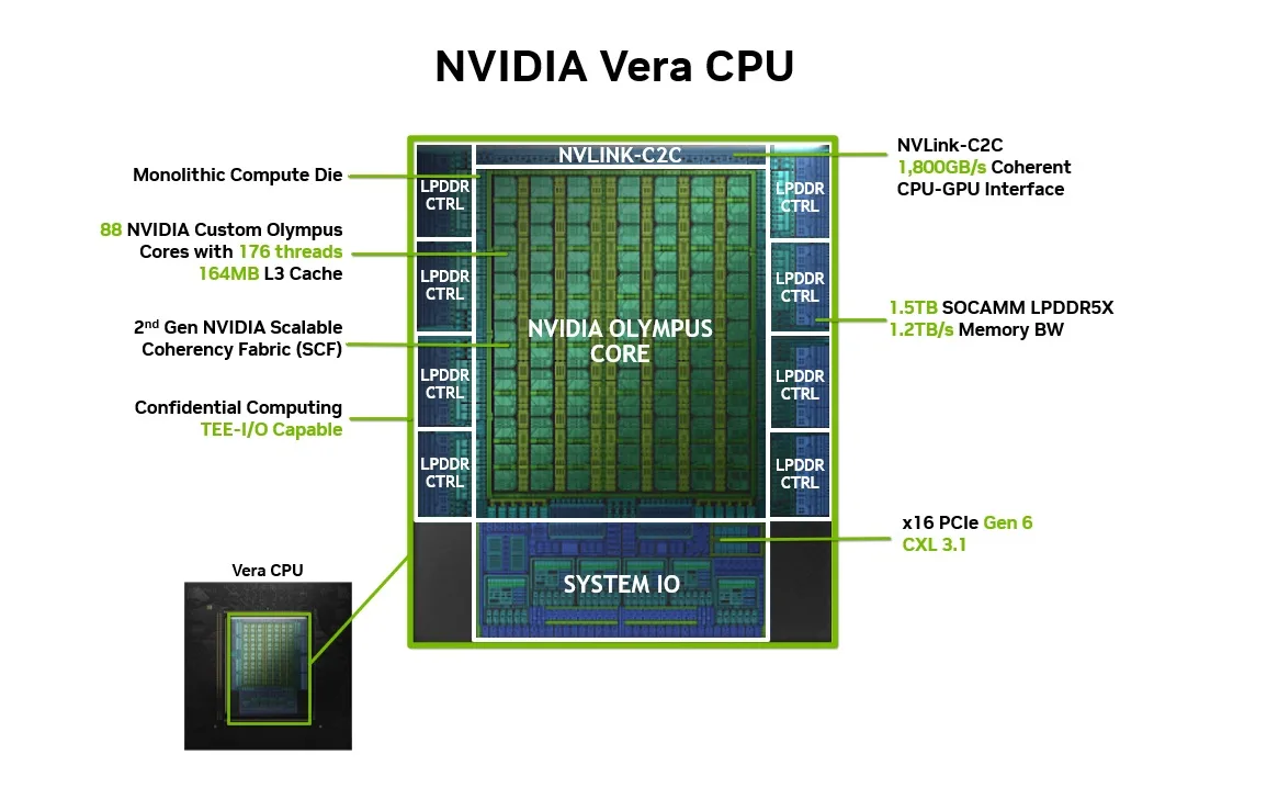
The 2nd-generation Scalable Coherency Fabric is the on-chip network that connects all 88 Olympus cores to the shared L3 cache and memory controllers.
- Built on a single monolithic compute die — Nvidia explicitly avoided chiplet boundaries on the compute side here.
- Why: chiplet boundaries add latency and bandwidth variability. For a CPU whose job is deterministic data movement at line rate, that variability is unacceptable.
- Result: SCF sustains over 90% of peak memory bandwidth under load, which means software actually sees close to the headline 1.2 TB/s figure rather than a fraction of it.
Note that Vera disaggregates memory controllers and I/O into chiplets (similar to Rubin), but keeps the compute die monolithic. The split reflects the engineering priority: chiplet-ize the parts that benefit from independent yield, keep monolithic the parts that need deterministic latency.
(4) I/O — NVLink-C2C, PCIe Gen6, CXL 3.1
Vera lifts every host-side I/O interface by 2× or introduces a new one. The comparison vs Grace:
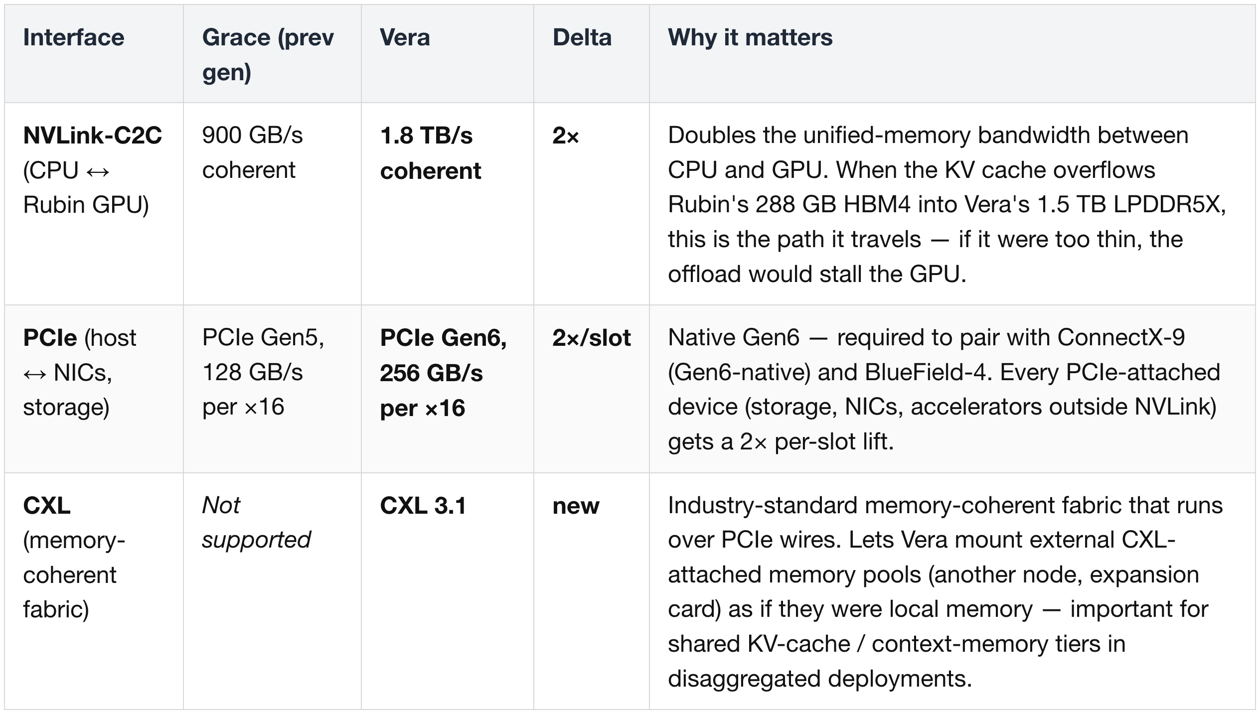
"Coherent" on the NVLink-C2C row means the CPU and GPU automatically see the same memory contents without explicit synchronization (covered in detail in Rubin section (4) of Part 2).
(5) The Vera Rubin Superchip
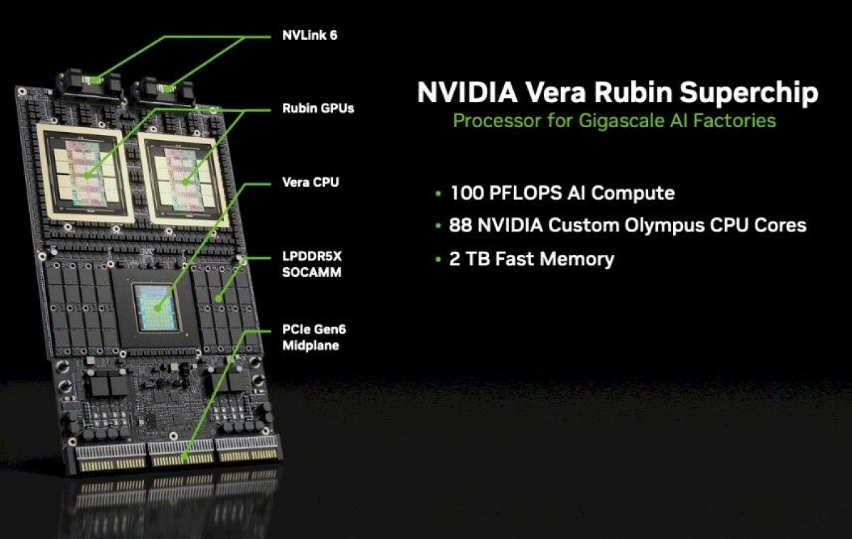
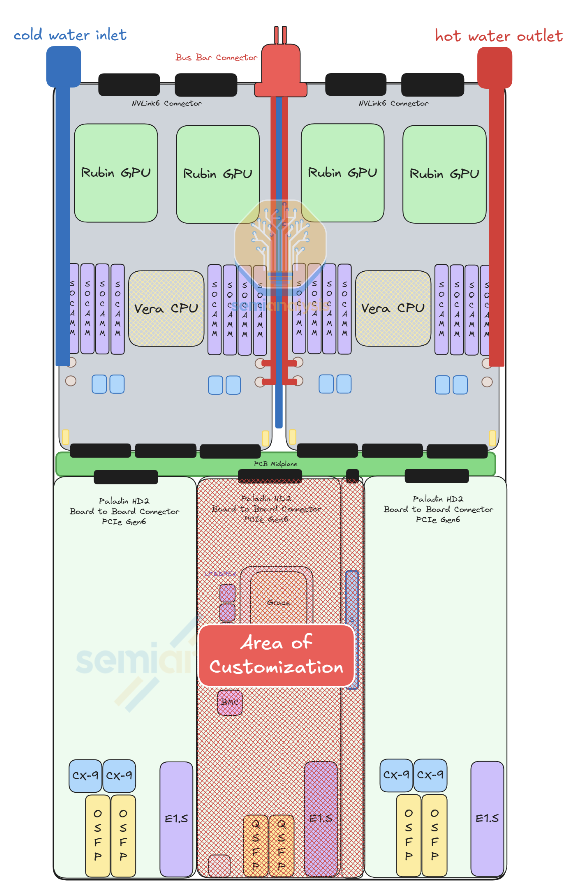
Vera is not sold as a standalone CPU in the typical case. The default deployment is the Vera Rubin Superchip: one Vera CPU + two Rubin GPUs, tightly coupled on a single host motherboard module.
- The CPU and both GPUs are connected via NVLink-C2C in a coherent memory domain.
- This is the fundamental compute building block of the NVL72 rack — each compute tray holds two superchips, and the rack holds 18 trays.
- Total per superchip: 100 PFLOPS NVFP4 (2× Rubin GPU), 2 TB of fast memory, 88 Olympus cores, ~6 T transistors across all silicon on the module.
Vera can also be deployed standalone for agentic processing, analytics, cloud, storage, and infrastructure services — but the superchip configuration is what drives the rack-scale platform thesis.
(6) Summary — Vera in One Read
The full spec-by-spec deltas (with engineering consequences) live in the upfront "Grace → Vera at a glance" tables. This section synthesizes the thesis behind them.
The cleanest read: Vera exists to make sure the CPU side never becomes the limiting factor in feeding a Rubin GPU. Every spec lift — bandwidth, capacity, coherent link width, custom core design — is calibrated to match the throughput of the GPU it pairs with.
5. NVLink 6 Switch
NVLink 6 Switch is the scale-up fabric chip of Vera Rubin — the silicon inside the rack-level NVLink switch trays that lets all 72 Rubin GPUs communicate as a single accelerator.
- "Scale-up" = building a larger virtual accelerator from many chips (within a rack).
- "Scale-out" = connecting many such racks across a datacenter (handled separately by ConnectX-9 + Spectrum-6).
- The NVLink Switch is to the rack what a CPU's on-die ring/mesh is to a multi-core chip — the all-to-all interconnect.

(1) The "Same Switch Chip, Twice the Rack" Trick
The deltas split into three layers: what changed inside the switch silicon, how the trays and rack aggregate that silicon, and what extra capability the switch now performs beyond pure switching.
Chip-Level Silicon
Tray + Rack Aggregation
In-Network Compute (SHARP)
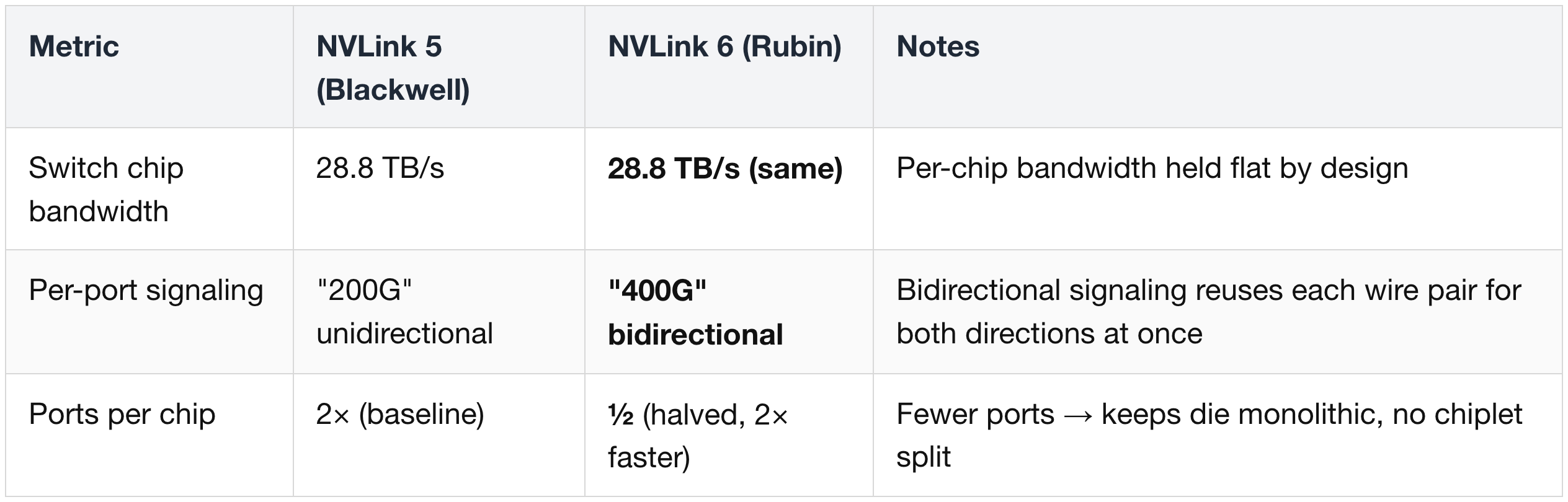
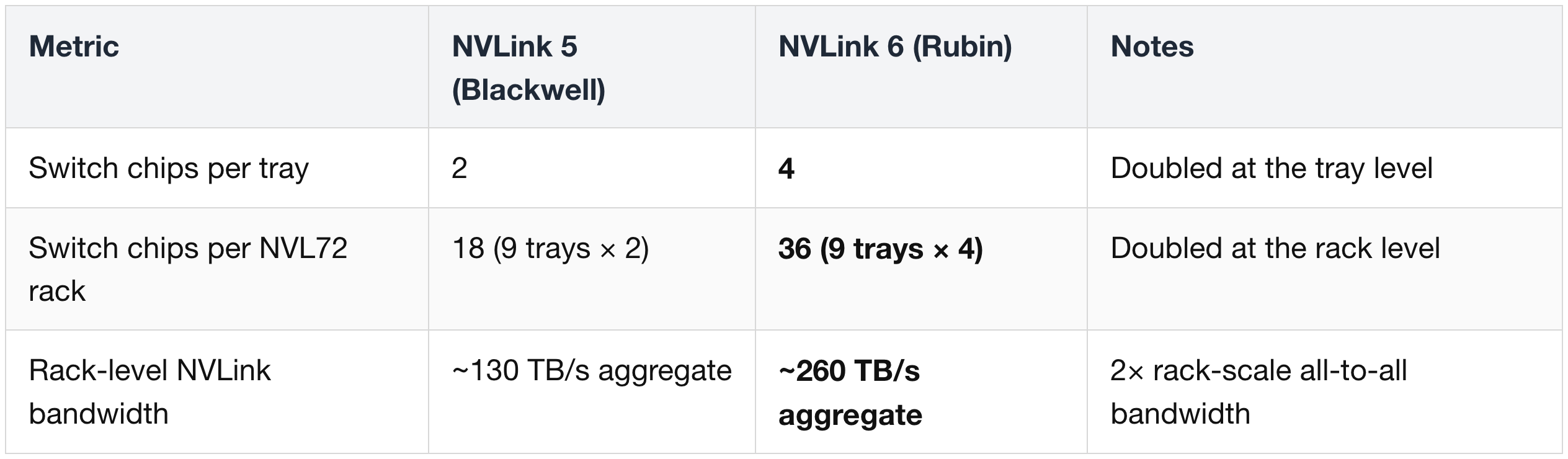
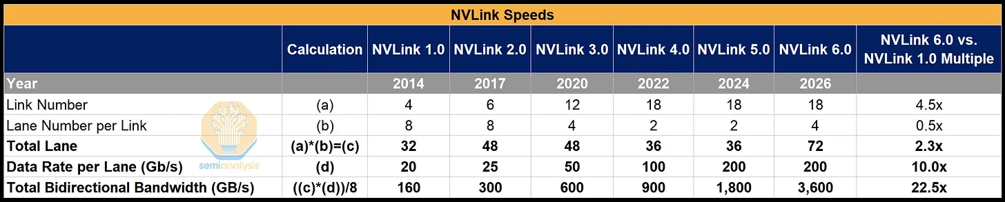
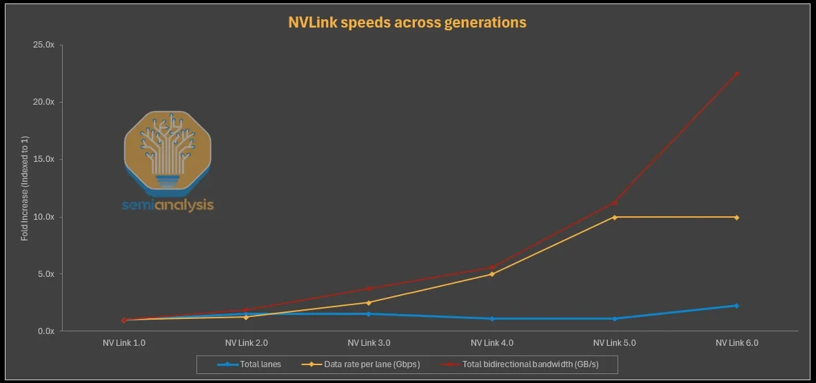
The key design choice: the chip-level 28.8 TB/s switching bandwidth was held constant between NVLink 5 and NVLink 6.
- Doubling chip-level bandwidth would have required either a bigger die or a multi-die switch — both expensive in design complexity.
- Instead, Nvidia kept the same chip throughput but doubled the per-link SerDes rate (via bidirectional signaling) and halved the port count.
- Rack-level 2× scaling then comes from doubling chips per tray (2 → 4), not changing the tray or rack form factor.
(2) Bidirectional SerDes — How NVLink 6 Doubles Per-Link Rate
The headline number is straightforward: NVLink 5 delivered 224G per electrical lane → NVLink 6 delivers 448G per electrical lane. A 2× per-lane jump.
The interesting question is how Nvidia got there without doubling the modulation rate or the baud rate — both of which would have required new SerDes silicon and tighter signal-integrity margins. The answer: simultaneous bidirectional signaling on the same copper wire pair.
Why simple "more cables" wasn't the answer
The naive way to double NVLink bandwidth would have been to keep the existing 200G SerDes and just double the number of copper cables on the backplane. Two reasons that doesn't work:
- The Blackwell NVL72 backplane already carries ~5,000 copper cables. Doubling that to ~10,000 cables is mechanically and thermally hard, and pushes the reliability failure modes that GB200/GB300 already exhibit much further.
- The alternative — going to a wider rack (as AMD does with its MI400 Helios rack) — extends PCB trace lengths, which degrades signal integrity at high speed.
So Nvidia kept the cable count flat and pushed the SerDes rate instead.
What "bidirectional" actually means
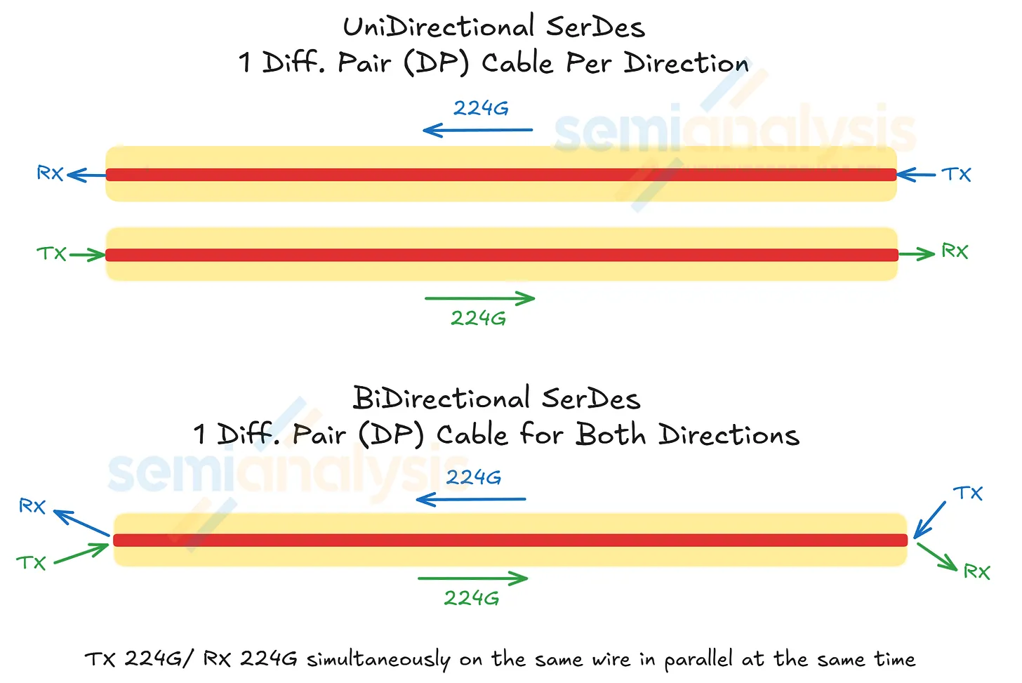
An NVLink electrical lane is one differential pair (DP) — two conductors carrying equal-magnitude, opposite-polarity signals. Traditionally, that pair carries a signal in one direction at a time. Bidirectional SerDes runs both directions simultaneously on the same pair.
The physics of the problem:
- In optics, you can solve this with an optical circulator — a passive device that routes the inbound and outbound light onto separate paths so they don't collide at the receiver. (Google's TPUv7 uses this approach for its optical interconnects.)
- In copper, you can't. Copper cables are linear transmission lines — the inbound and outbound signals simply sum at the receiver via superposition. So the local receiver sees its own outbound signal mixed with the remote transmitter's inbound signal.
The "hybrid" + echo-cancellation trick
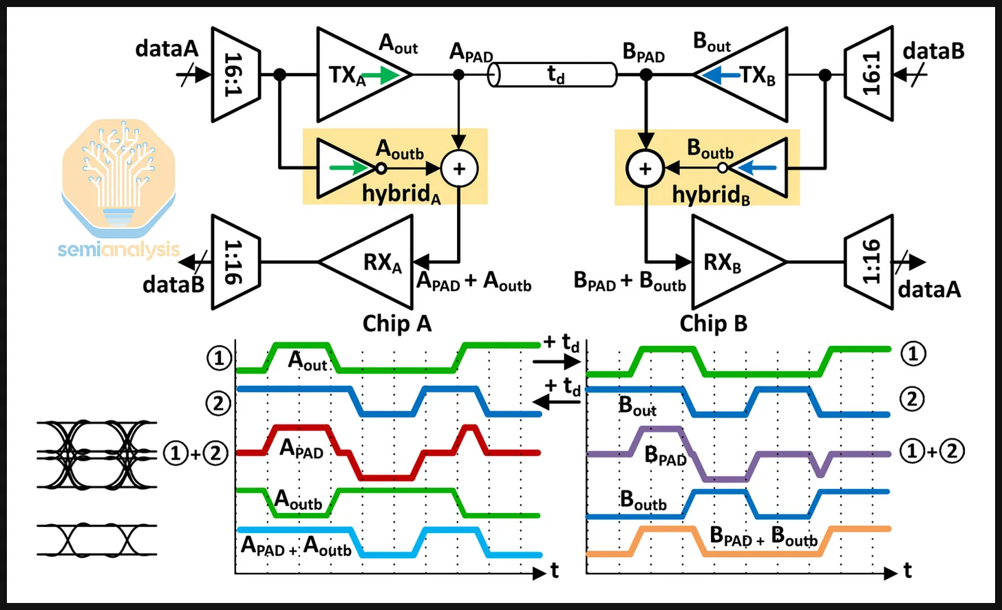
The solution is a hybrid circuit at each end of the wire plus echo cancellation:
- Without echo cancellation, the local receiver sees:
(remote TX) + (local TX) = garbage. - The hybrid generates an inverted copy of the local TX and injects it at the local RX node.
- Result:
(remote TX) + (local TX) + (−local TX) = (remote TX)— the local TX cancels itself out, leaving only the remote signal.
In short, each end subtracts its own transmission from what it's receiving in real time, leaving only what the other end actually sent.
Why this is hard in practice
- Echo cancellation must be precisely calibrated. If the inverted TX copy is delayed even slightly relative to the actual TX leaking back into the receiver, the cancellation is imperfect and the link fails.
- This calibration has to hold across temperature variation, voltage variation, and aging of the silicon.
- Bidirectional signaling has been used for very short-reach (under 5 mm) die-to-die interconnects for years. What's notable about NVLink 6 is extending the same technique to the rack-scale copper backplane at reaches of at least 1 m. That's a substantial engineering leap.
What you get
- Same number of copper cables on the backplane as NVLink 5
- 2× per-link bandwidth (224G → 448G per differential pair)
- Same NVLink Switch chip floorplan (no need to widen the die)
- The chassis, backplane, and connector mechanical infrastructure (Amphenol's PaladinHD2 family) carry over with minimal change
The trade-off is reliability margin — bidirectional links are more sensitive to calibration drift, so the link-error correction and retry layers have to be more robust. So far, Nvidia is shipping bidirectional NVLink 6 in volume, so the engineering is holding up at the manufacturing scale required.
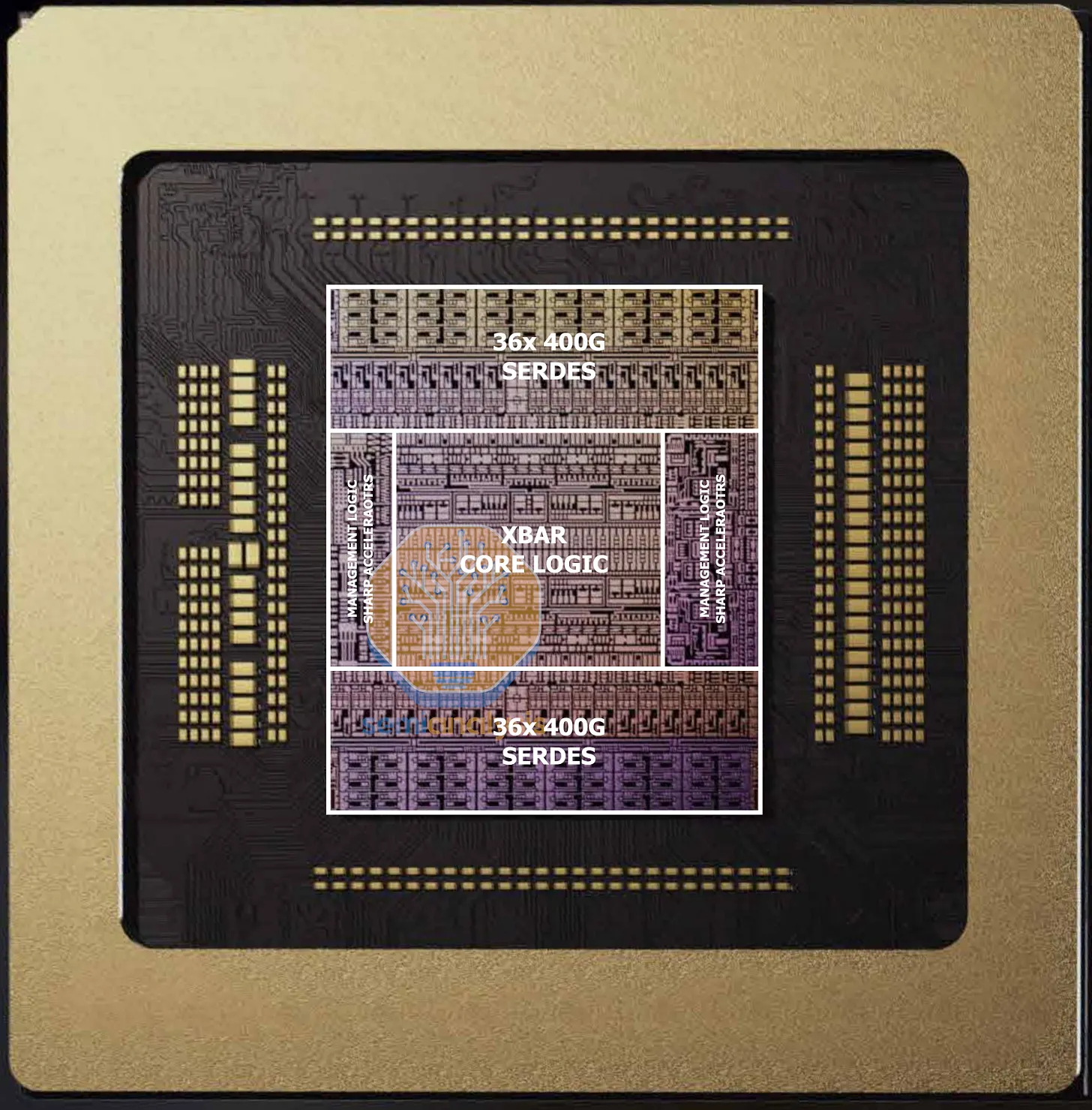
(3) Die Layout
The internal floorplan is unchanged from NVLink 5:
- Two sides of the die handle IO (the SerDes lanes connecting to GPUs and to other switch chips).
- A central logic section is the crossbar — the matrix that routes any input to any output.
- SHARP in-network compute is embedded in that central region, running collective math (sum, reduce, broadcast) on data as it passes through.
Keeping the layout familiar means much of the validated NVLink 5 design infrastructure (timing closure, physical implementation) carries over — important when the 3nm production schedule is already tight.
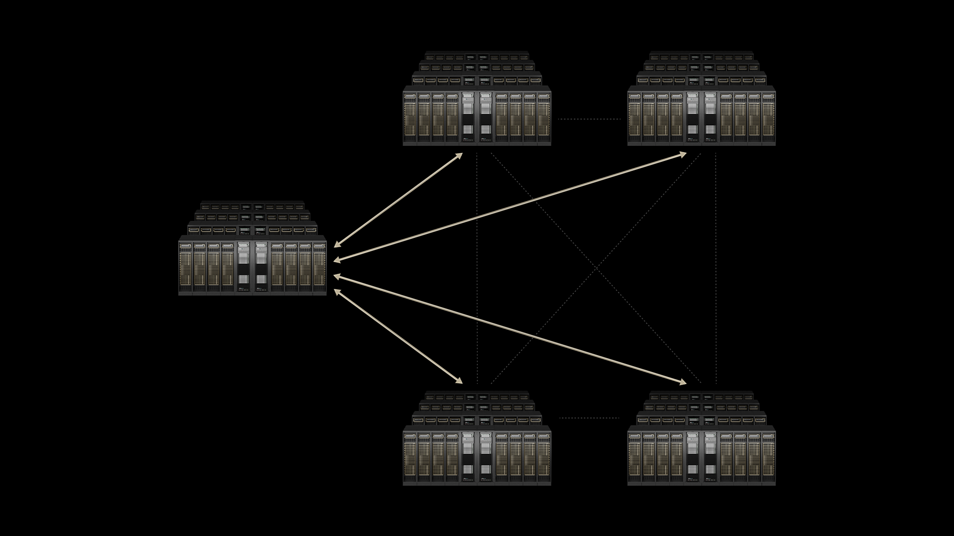
(4) All-to-all Topology & MoE Workloads

The 72 GPUs in an NVL72 rack are connected through the 36 NVLink 6 switch chips in a full all-to-all topology:
- Any GPU can talk to any other GPU at full 3.6 TB/s bandwidth.
- Single-hop latency — no hierarchical aggregation, no hotspots, no hop-dependent variance.
- From software's point of view, the rack is one accelerator.
Why this matters for MoE (Mixture-of-Experts)
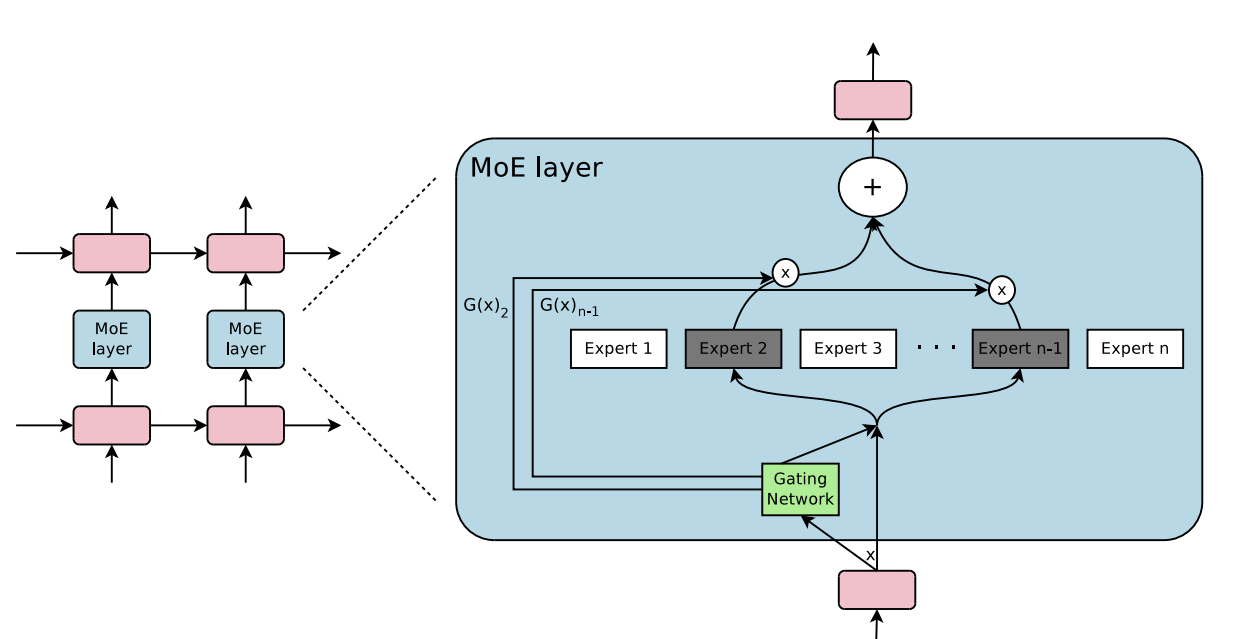
MoE models split work across many "expert" sub-networks. During each token's forward pass:
- A router decides which experts each token goes to.
- Tokens get dispatched across GPUs — every GPU may need to send some tokens to every other GPU (the "all-to-all" pattern).
- Then results get gathered back the same way.
This is one of the most bandwidth-stressful traffic patterns in modern AI. On a hierarchical fabric (e.g., GPUs grouped into "domains" connected through fewer uplinks), all-to-all saturates the uplinks and bottlenecks the workload. A flat all-to-all fabric like NVLink 6 keeps every GPU pair at full bandwidth, which is why Nvidia reports 2× higher all-to-all throughput for MoE inference vs NVLink 5.
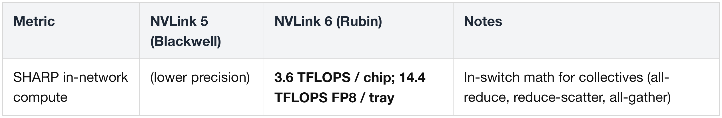
(5) SHARP — Doing Math Inside the Switch
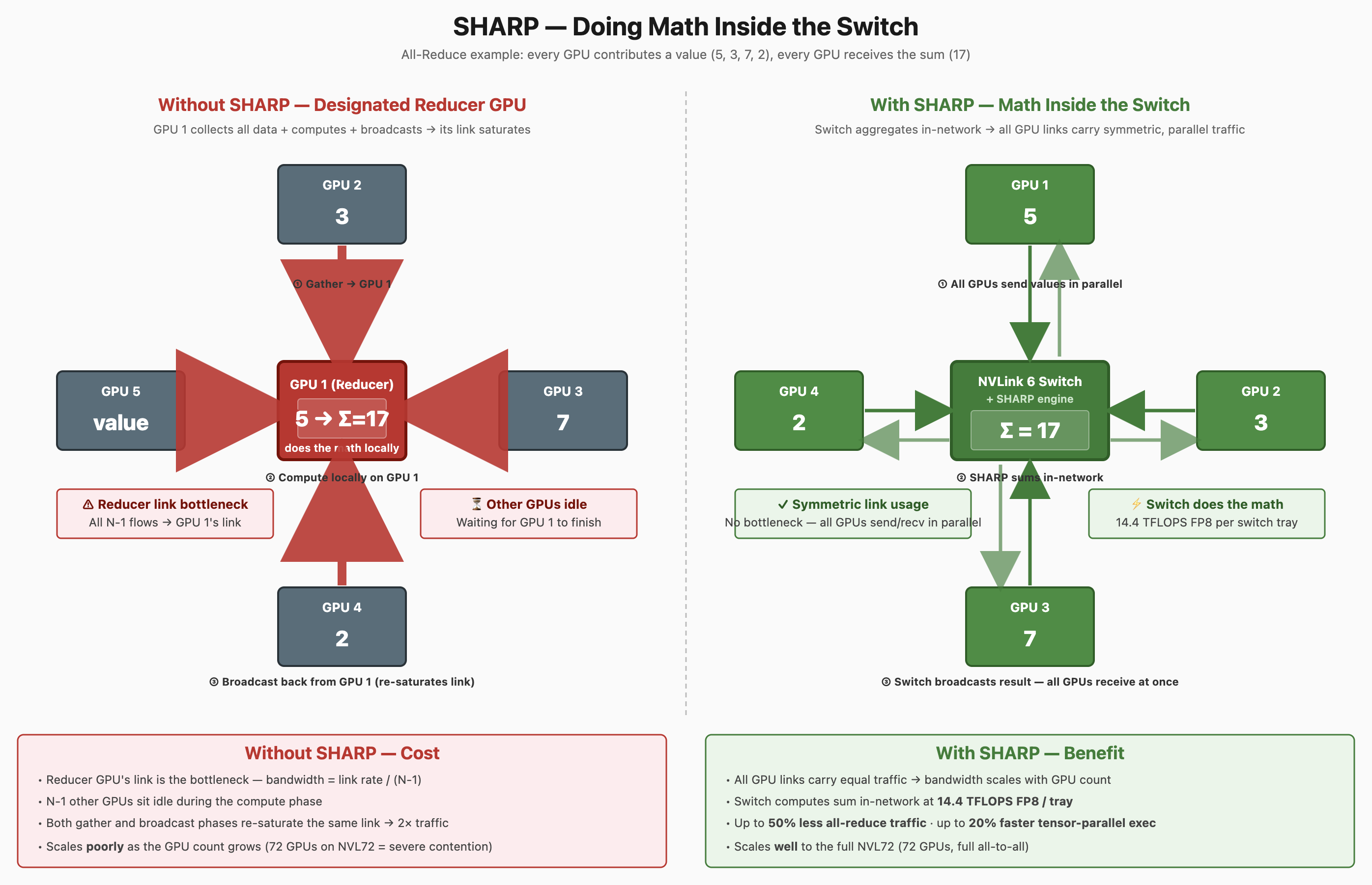
SHARP (Scalable Hierarchical Aggregation and Reduction Protocol) puts compute inside the switch silicon rather than only inside the GPU.
The pattern it accelerates:
- Training collectives — all-reduce, reduce-scatter, all-gather — require every GPU's contribution to be summed (or aggregated) and the result returned to every GPU.
- Without SHARP: every GPU sends data to a designated reducer GPU, which sums it and broadcasts back. The reducer GPU's link saturates, and the others sit idle waiting.
- With SHARP: the switch itself sums data as it passes through. The aggregated result emerges at every output without any GPU acting as a bottleneck.
Per-tray throughput:
- 14.4 TFLOPS of FP8 in-network compute per switch tray (4 chips × 3.6 TFLOPS each).
- Nvidia claims SHARP can reduce all-reduce communication traffic by up to 50% and improve tensor-parallel execution time by up to 20% at scale.
(6) Operability — Hot-swap, Telemetry, Partial Rack
NVLink switches must be operable at AI factory scale, not just fast:
- Hot-swappable switch trays — replace a failed tray without draining the rack.
- Partial-population support — the rack can run with fewer than 9 switch trays during maintenance.
- Dynamic traffic rerouting when a switch chip or link goes offline.
- In-service software updates without taking the rack down.
- Fine-grained link telemetry streamed through the switch interfaces for real-time monitoring.
These features matter because at the cost of an NVL72 rack ($3M+), unplanned downtime is the binding constraint, not raw bandwidth.
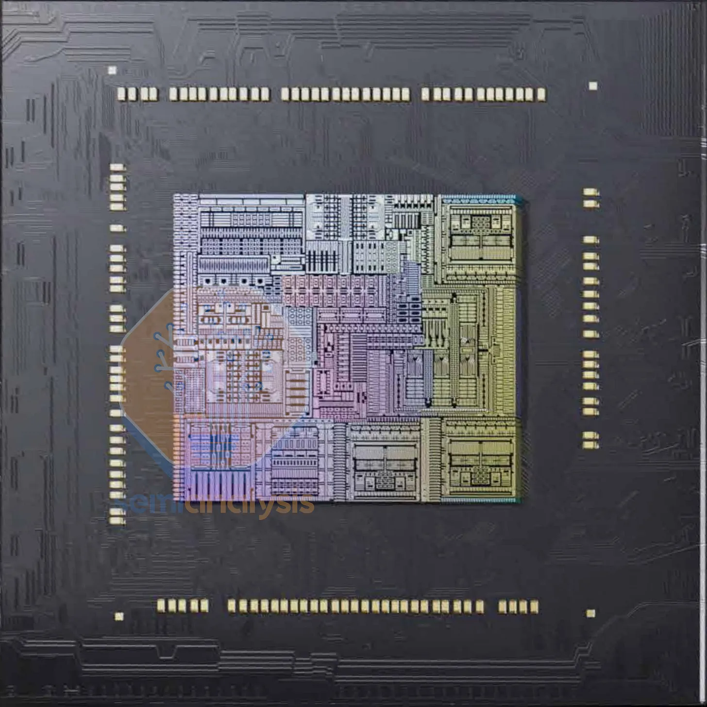
6. ConnectX-9
ConnectX-9 (CX-9) is Nvidia's scale-out network interface card (NIC) — the chip that plugs each GPU into the Ethernet or InfiniBand fabric extending beyond the rack. Where NVLink 6 connects the 72 GPUs inside an NVL72, ConnectX-9 connects each NVL72 to the rest of the datacenter.

(1) Mostly Iterative from ConnectX-8
ConnectX-9 is a deliberate, conservative iteration on ConnectX-8 — same generation of process and same headline bandwidth, with selective upgrades. The deltas split cleanly into two layers: what the NIC silicon itself does (largely unchanged) and how it's deployed in the Vera Rubin system (doubled).
NIC Silicon (per chip)
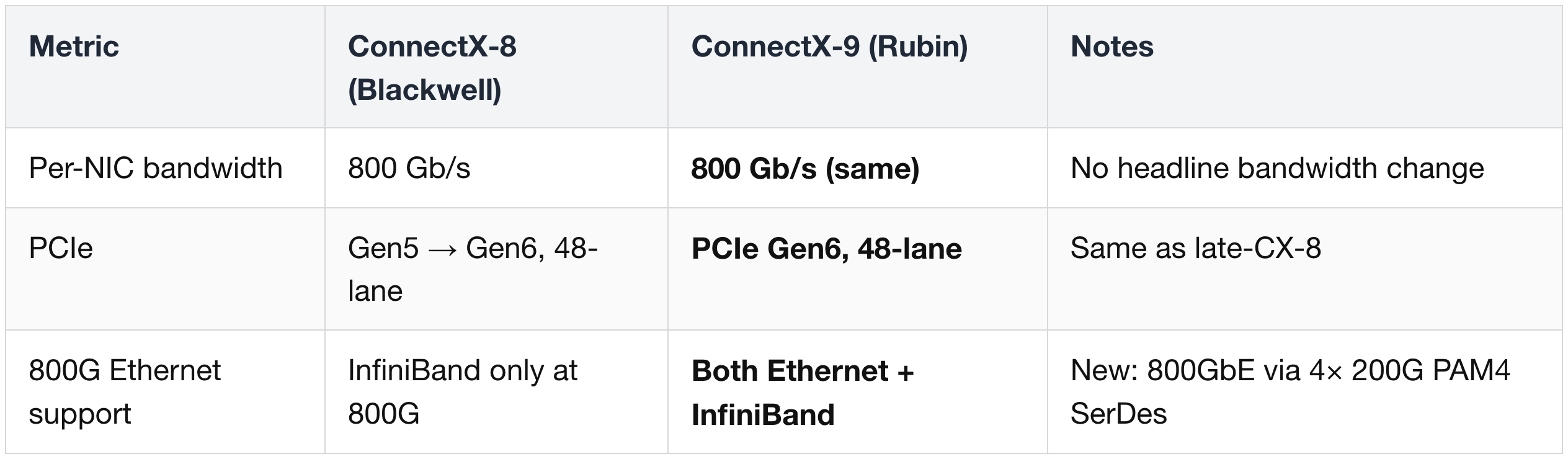
Platform Deployment (per GPU)
The pattern is clear: scale-out bandwidth doubles per GPU, but the NIC silicon itself does not. Nvidia got the 2× scale-out story by doubling the number of NICs per GPU, not by spending engineering effort on a new tape-out.
(2) The "800G Ethernet" Detail That Matters
ConnectX-8 supported 800G only on the InfiniBand protocol. On Ethernet, it topped out at 400G.
- ConnectX-9 closes this gap: 800G Ethernet via 4 × 200G PAM4 SerDes.
- PAM4 (Pulse Amplitude Modulation, 4 levels) encodes 2 bits per signal symbol, doubling effective rate over basic NRZ signaling at the same physical clock.
- This matters because most hyperscalers prefer Ethernet (open ecosystem, lower switch cost) over InfiniBand for scale-out. Until CX-9, an 800G Ethernet GPU NIC didn't exist in Nvidia's lineup.
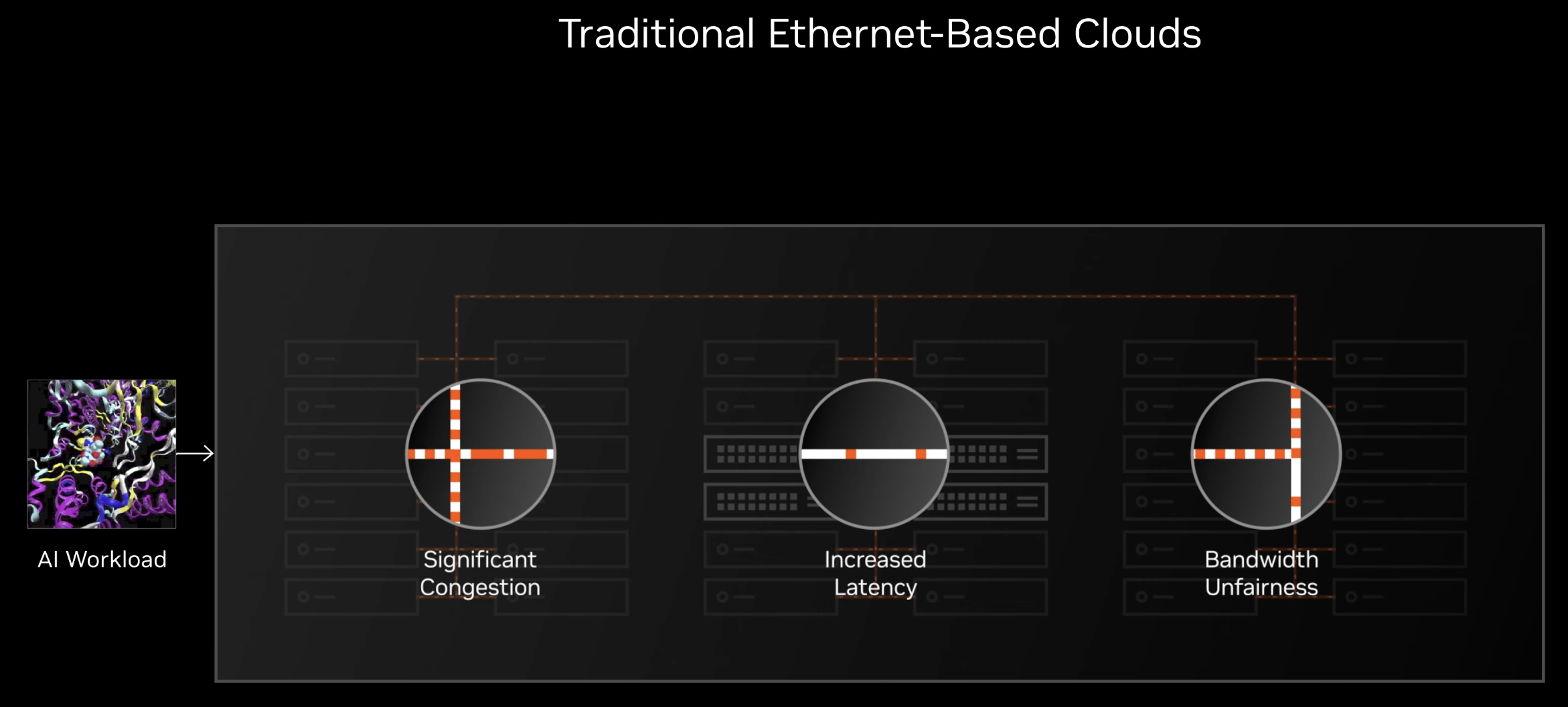
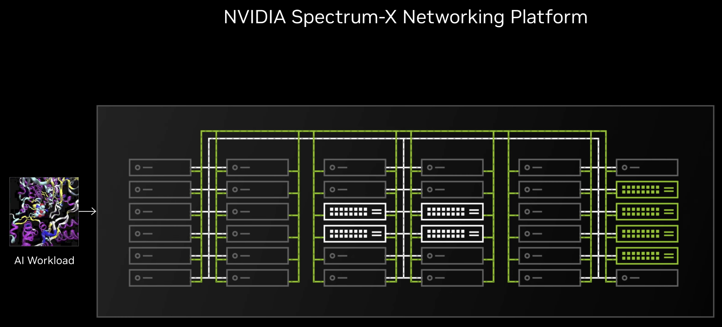
(3) Endpoint-Level Congestion Control
ConnectX-9's most engineering-interesting feature is what it does before packets enter the fabric:
- AI traffic patterns are highly correlated — many GPUs inject data into the network at the same time (e.g., during the all-to-all phase of MoE inference).
- Traditional NICs are passive: they fire packets into the network and let switches handle congestion after it forms.
ConnectX-9 instead enforces endpoint-level control through:
- Programmable congestion control, which dynamically adjusts packet transmission rates, retransmission behavior, and prioritization in software when the network becomes congested;
- Traffic shaping, which smooths outbound traffic flows and reduces burstiness by regulating how quickly packets are sent;
- Packet scheduling, which determines the order in which different packet types are transmitted — for example, prioritizing latency-sensitive traffic while delaying lower-priority flows.
The result:
- Bursty traffic injections are smoothed at the endpoint before reaching the scale-out switch.
- Head-of-line blocking is reduced, as traffic queues are less likely to be clogged by sudden bursts.
- “Victim flows” are mitigated, meaning one tenant’s burst is less likely to hurt another tenant’s throughput.
- Effective bandwidth remains high under load, instead of collapsing during congestion events.
(4) Multi-Tenant Isolation
ConnectX-9 enforces per-tenant fairness and isolation at the endpoint.
- As a result, each compute task experiences a more predictable network flow, even when sharing the same scale-out fabric with other compute tasks, regardless of their traffic patterns.
- Enforcing isolation at the endpoint scales better than switch-only QoS, because every switch in the fabric does not need to track every individual data flow.
- Here, QoS refers to Quality of Service — a network control mechanism that manages traffic priority, bandwidth allocation, and latency so that no single compute task or tenant consumes excessive bandwidth or blocks other traffic on the shared scale-out fabric.
- As a result, cross-tenant interference is reduced, where congested traffic from one tenant degrades another tenant’s throughput or latency.
In other words, ConnectX-9 moves part of the isolation logic in a multi-tenant AI fabric toward the GPU server endpoint, making network behavior more predictable and scalable.
7. BlueField-4
BlueField-4 (BF-4) is a data processing unit (DPU) — a chip that runs the infrastructure layer of the AI factory: networking control plane, storage I/O, security, telemetry, orchestration.
The idea: take all the work that traditionally runs on the host CPU (the OS-level plumbing for handling network packets, storage requests, security checks, etc.) and move it onto a dedicated chip. The host CPU and GPU then spend 100% of their cycles on application work.

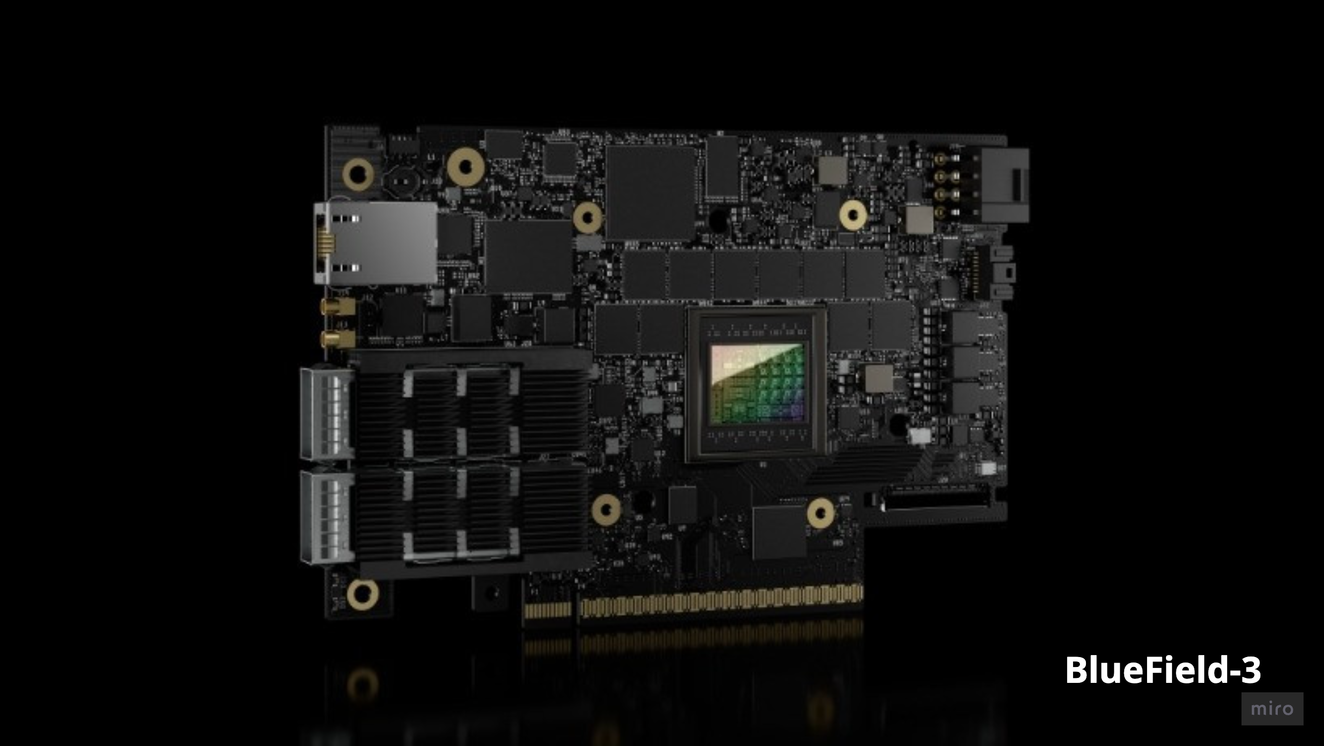
(1) The Big Design Change vs BlueField-3
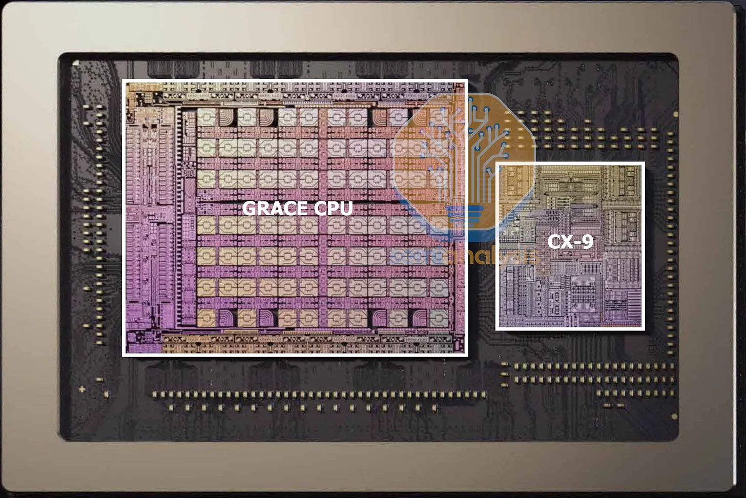
BlueField-4 abandons the bespoke-tapeout approach used in BF-3 and instead packages two existing dies together:
- One Grace CPU die (Nvidia's previous-generation 72-core ARM CPU — yes, the same Grace from GB200, not the new Vera)
- One ConnectX-9 die (the same NIC chip used as a discrete NIC in the rest of the system)
This is a "chiplet reuse" strategy — package two already-validated dies together rather than designing new silicon. It explains why BF-4's compute side is essentially a Grace CPU, and why its networking side is a CX-9.
The deltas track the dual-die structure of BF-4: the Grace-CPU die contributes compute + memory, the ConnectX-9 die contributes networking, and both together accelerate the security + storage workloads the DPU is designed to run off-host.
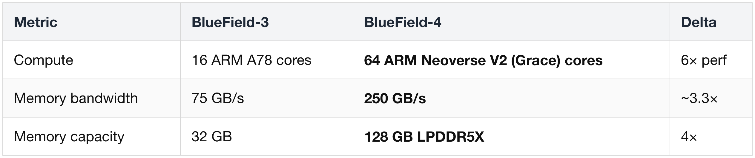
Compute & Memory (Grace-CPU side)
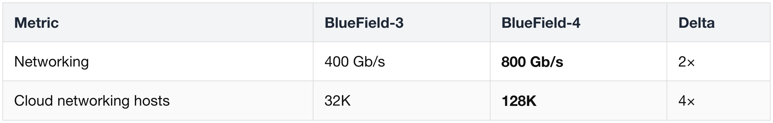
Networking (ConnectX-9 side)
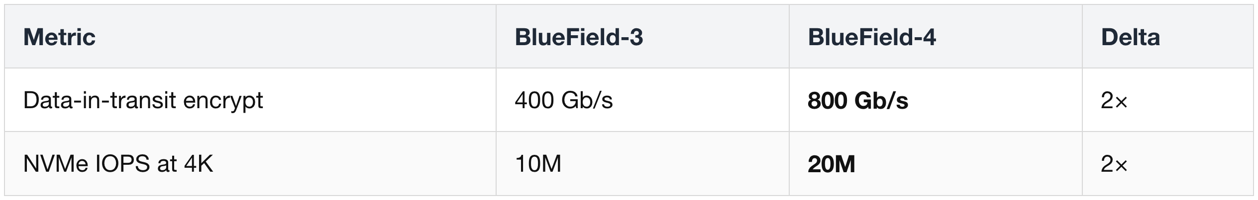
Security & Storage Acceleration
Note: the 128 GB of LPDDR5X on BF-4 runs at roughly half the bandwidth of regular Grace — BF-4 doesn't need the full Grace memory subsystem (it's a control-plane chip, not a primary compute engine), so the memory configuration is dialed back.
(2) What BF-4 Actually Does in a Rubin Compute Tray
Inside a VR NVL72 compute tray, BF-4 sits at the front-center of the chassis and handles the following functions:
- Front-end (north-south) networking — connecting the compute tray to the datacenter network, including external clients, the datacenter fabric, storage systems, and management servers.
- Storage controller functions — terminating NVMe-over-Fabrics (NVMe-oF), a storage protocol that allows NVMe SSDs to be accessed remotely over a network fabric such as Ethernet or InfiniBand instead of being directly attached to the server via PCIe, as well as other storage protocols at line rate.
- Security — AES-XTS encryption at 800 Gb/s, threat detection, secure boot, and attestation.
- Telemetry & orchestration — collecting per-tray performance data and enforcing isolation between tenants.
The compute tray reference design has one BF-4 per tray, sitting between the left-side Orchid (CX-9) module and the management module. Onboard it carries 128 GB of LPDDR5X, 512 GB of pluggable SSD, and an AST2600 BMC (Baseboard Management Controller) for low-level board management.
(3) Adoption Reality — Most Hyperscalers Won't Use It
This is a commercial detail worth noting:
- BF-4 is expensive (a full Grace die + a full CX-9 die in one package, plus LPDDR5X, plus SSD).
- Most hyperscalers (AWS, Google, Microsoft, Meta) already have in-house DPU designs for their existing fleets.
- For them, the BF-4 slot in the compute tray will be replaced by either an in-house DPU or simply a bare CX-9 NIC (cheaper, no compute-side overhead).
- BF-4 will primarily ship to smaller neoclouds with less customization capability (CoreWeave is the canonical example).
This is the same pattern as BF-3: technically impressive, but the addressable market is narrower than Nvidia's marketing implies.
(4) ICMS — The "Third Network" Built Around BF-4
BlueField-4 is the silicon anchor of ICMS (Inference Context Memory Storage, possibly to be rebranded "CMX" at GTC) — a new memory tier specifically for KV cache offload at petabyte scale.
What ICMS is
- A purpose-built KV cache fabric sitting between GPU HBM (Tier 1), Vera LPDDR5X (Tier 2), and durable storage (Tier 4).
- Nvidia calls this the "G3.5" tier — Ethernet-attached, flash-based, optimized for ephemeral, latency-sensitive KV cache.
- Sized for petabytes of shared capacity per GPU pod.
Why a third network exists
- Long-context inference (millions of tokens) and multi-agent workflows generate KV caches that:
- Overflow GPU HBM and even Vera LPDDR5X.
- Are reusable across requests (so re-computing is wasteful).
- Need much faster access than durable storage.
- ICMS turns these into a shared pod resource — KV cache becomes a first-class infrastructure tier.
BF-4’s role specifically in the ICMS context
In the ICMS architecture, BF-4 acts as the dedicated controller for the KV cache data path, rather than a generic storage NIC. Its role is to move latency-sensitive KV cache blocks between Rubin GPUs and the ICMS flash tier while offloading protocol handling, data movement, integrity checks, and security from the host CPU and GPU.
- Runs the KV I/O plane
BF-4 executes the dedicated I/O path for KV cache traffic. This includes terminating NVMe-oF and object/RDMA protocols at line rate, meaning the DPU directly interprets and processes these storage/network requests without pushing the full protocol workload back to the host CPU. - Moves KV data without host CPU or GPU involvement
BF-4 transfers KV cache data between Rubin GPUs and the ICMS flash tier without requiring heavy intervention from the host CPU or GPU. This reduces CPU serialization, memory-copy overhead, and tail-latency spikes that could otherwise stall inference decode. - Acts as a KV cache storage controller
Within ICMS, BF-4 functions as a storage controller, RDMA endpoint, protocol terminator, encryption engine, and data-integrity engine for KV cache traffic. In other words, it treats KV cache not as ordinary storage data, but as latency-sensitive inference memory. - Four BF-4 chips per Context Memory Storage system
Each Context Memory Storage system includes four BF-4 chips, allowing the system to scale KV cache movement across the ICMS flash tier while maintaining high throughput and low-latency access. - Dedicated BF-4 for KV cache traffic in DGX-style deployments
In a preferred DGX-style deployment, one BF-4 per tray is dedicated purely to KV cache traffic and is not shared with generic storage I/O. This prevents ordinary storage traffic, such as checkpointing, logging, or dataset reads, from interfering with latency-sensitive KV cache access.
In short, BF-4 is the control and data-movement engine that lets ICMS behave like a dedicated KV cache memory tier between GPU HBM and conventional shared storage.
(5) ASTRA — BF-4 as the Tray's Trust Anchor
- ASTRA as the tray-level trust framework
ASTRA is the trust and control framework inside Vera Rubin NVL72 that moves infrastructure control away from the tenant-controlled host environment and anchors it inside the BlueField-4 DPU. - BF-4 as the silicon trust anchor
BF-4 provisions, isolates, configures, and monitors tray-level infrastructure resources through a DPU-managed control plane, rather than relying on the host CPU or tenant OS. - BF-4–to–ConnectX-9 control path
Through dedicated links to ConnectX-9 SuperNICs, BF-4 can program and enforce network policies across both the N-S front-end network and the E-W AI compute fabric. - Tenant access limited to the data path
Tenants can use the SuperNIC data path for high-performance AI communication, but cannot access or modify the SuperNIC control plane. - Policy enforcement on the DPU/SuperNIC layer
Network provisioning, tenant isolation, QoS policies, and fabric-level controls remain isolated on BF-4 and are enforced directly in SuperNIC hardware. - ASTRA vs. rack-scale TEE
ASTRA provides per-tray trusted infrastructure control, while rack-scale TEE (Trusted Execution Environment) extends confidentiality and integrity across the broader rack through CPU/GPU trust, NVLink encryption, secure device I/O, and remote attestation. - Core distinction
ASTRA secures who controls the tray; rack-scale TEE secures how workloads and data remain protected across the rack.
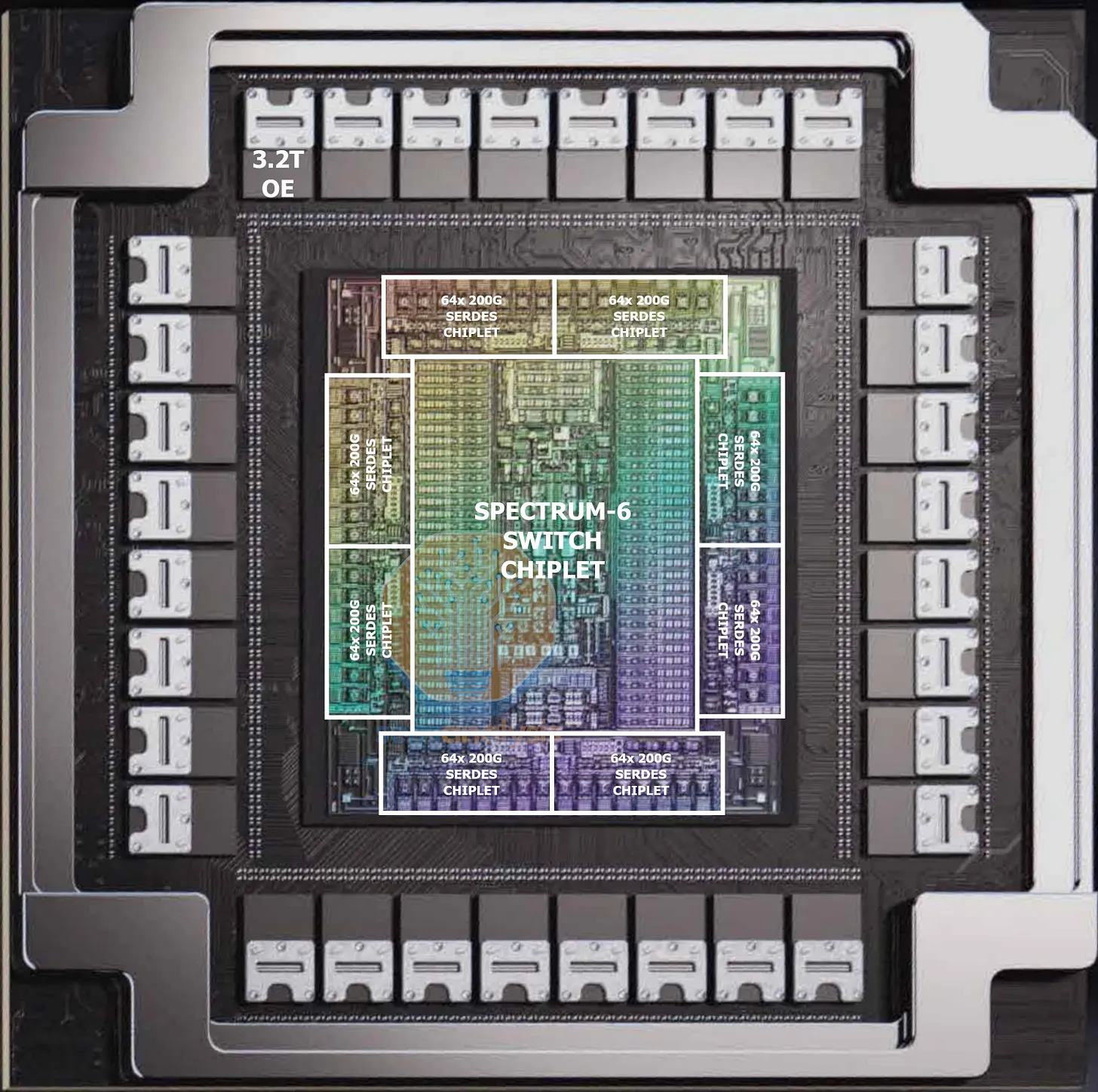
8. Spectrum-6
- Spectrum-6 is the Ethernet switch chip for connecting NVL72 racks together — and for connecting AI factories across geographic sites.
- It is not part of the NVL72 rack itself (NVLink 6 handles inside-rack traffic). Spectrum-6 lives in top-of-rack and aggregation switches that knit racks into a cluster.

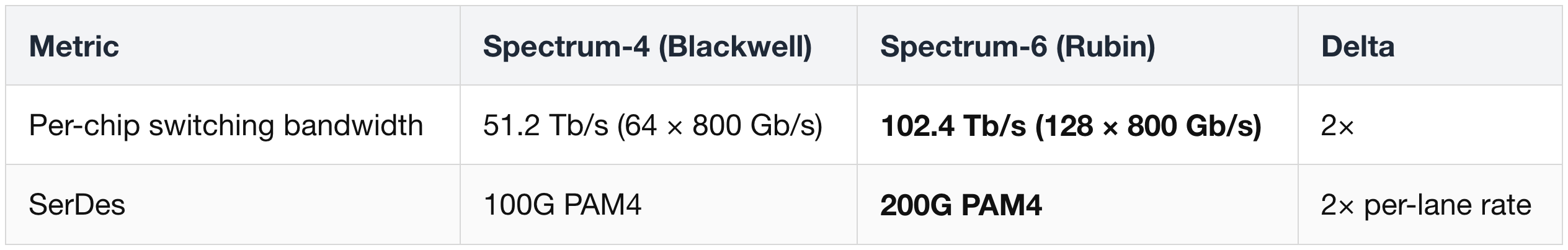
(1) Spectrum-4 → Spectrum-6 — Bandwidth Doubled
The deltas split into two layers: what the switch silicon itself does (bandwidth and signaling), and how that silicon gets packaged for deployment (optics integration and SKU choices).
Switch Silicon (per chip)
Package & Optics Integration
The 2× per-chip bandwidth comes from doubling the per-lane SerDes rate to 200G — not from a wider die. The chip layout (8 IO chiplets surrounding a central switch die) is unchanged from Spectrum-5.
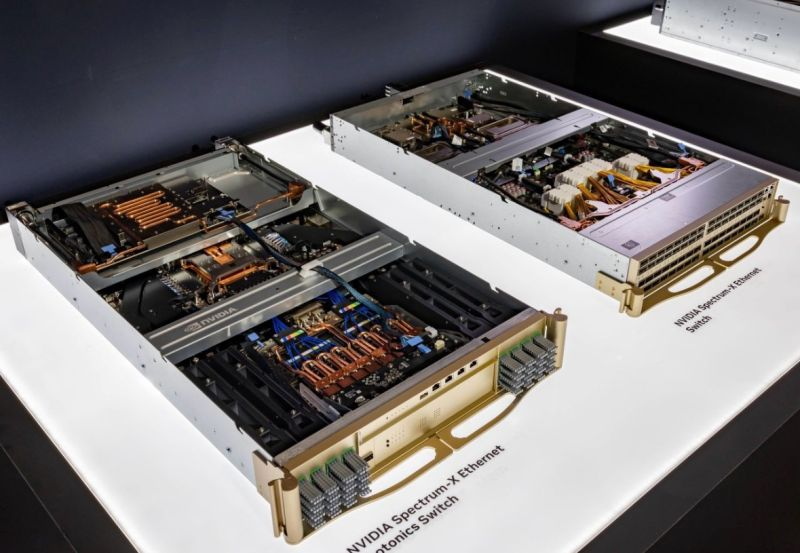
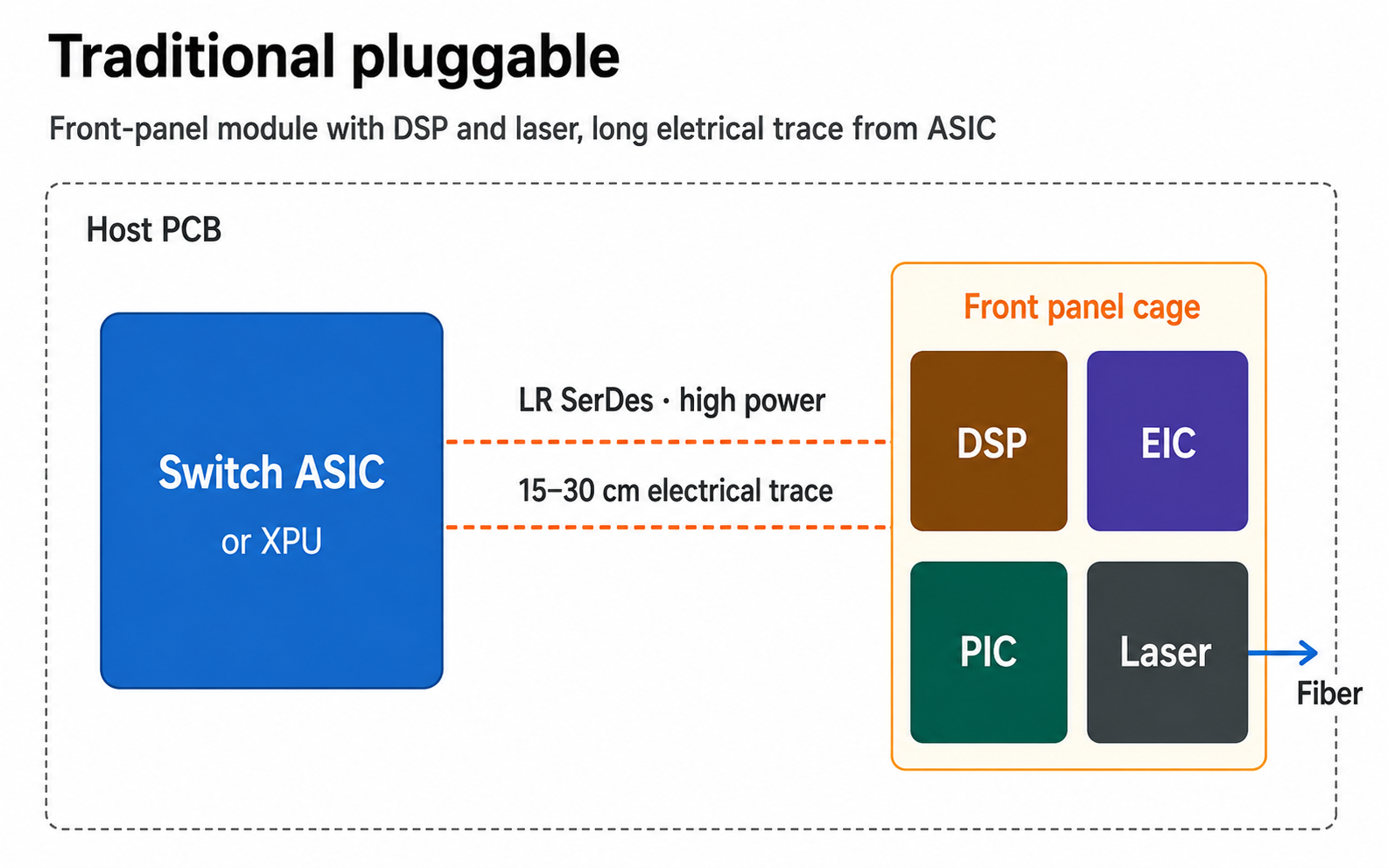
(2) Co-Packaged Optics (CPO) — Putting Optics Inside the Switch
Traditional Ethernet switches send electrical signals from the switch chip out to pluggable optical transceivers on the front panel. The transceivers convert electrical → optical, and the optical signals go out over fiber.
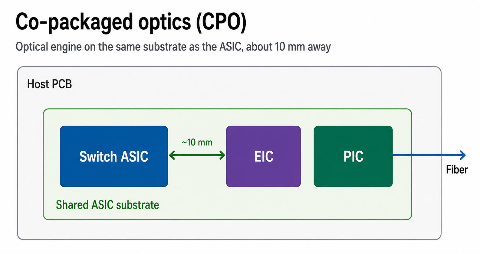
Spectrum-6 with CPO eliminates the pluggable transceivers and moves the optical engines inside the switch package itself:
- 32 silicon-photonics optical engines sit on the Spectrum-6 package, each delivering 3.2 Tb/s.
- The optical engines convert electrical signals to optical directly on the package.
- Detachable fiber connectors at the package edge plug straight into the fiber plant.
- External laser arrays provide the light source (lasers don't sit inside the package, for thermal/reliability reasons).
Why CPO matters
- ~5× better network power efficiency — eliminating long electrical traces and DSP retimers cuts power significantly.
- ~22 dB → ~4 dB optical loss reduction = up to 64× better signal integrity.
- Fewer failure points — pluggable transceivers are one of the most common failure modes in large datacenters.
- Lower end-to-end latency — no DSP retimers in the path.
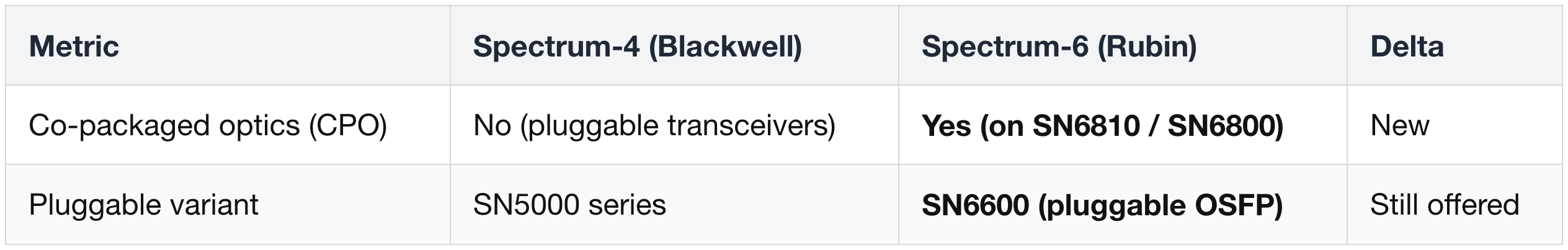
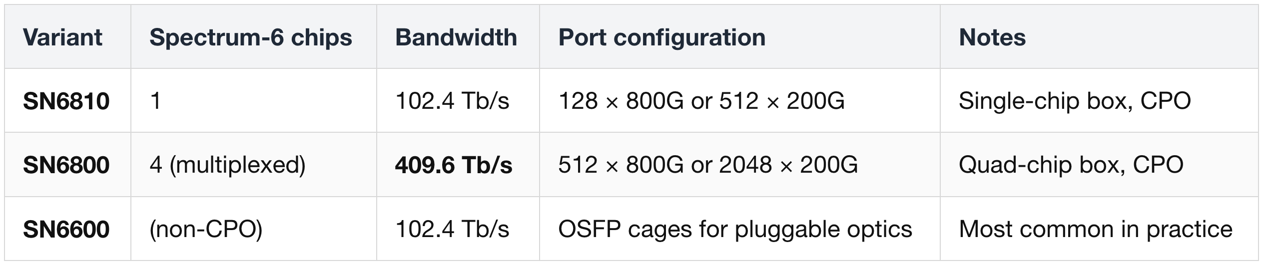
(3) Two Box Variants — SN6810 vs SN6800
Nvidia ships Spectrum-6 in two switch boxes:
Both CPO boxes are liquid-cooled.
Important commercial note
- The non-CPO SN6600 is expected to be the more common deployment — pluggable optics remain familiar, replaceable, and don't require Nvidia's CPO supply chain.
- CPO is the technically superior path but adopters need to be ready for the supply-chain and serviceability implications.
(4) Spectrum-X — Why a Custom Ethernet Stack
Spectrum-6 is just the chip. Spectrum-X is the full Ethernet fabric stack Nvidia built around it:
- Coordinated congestion control across switches and ConnectX-9 endpoints.
- Adaptive routing that reacts to live link conditions instead of static load-balancing hashes.
- Lossless Ethernet behavior through hardware-level flow control.
- End-to-end telemetry for fine-grained visibility.
The reason for all of this: off-the-shelf Ethernet was designed for enterprise traffic — many uncorrelated flows of different sizes.
- AI traffic is the opposite — synchronized, bursty, asymmetric, dominated by all-to-all collectives.
- Standard Ethernet packet loss / congestion mechanisms collapse under sustained AI load; Spectrum-X is engineered around the actual traffic shape.
Nvidia reports up to 3× faster job completion for variable all-to-all workloads on Spectrum-X versus off-the-shelf Ethernet.
(5) Spectrum-XGS — Scale-Across (Multi-site)
Spectrum-X also incorporates Spectrum-XGS (Ethernet scale-across):
- Adds distance-aware congestion control for AI deployments that span geographically distributed datacenters.
- Different latency regimes than single-site (round-trip times in tens of ms vs μs).
- End-to-end telemetry and deterministic routing balance load across sites.
This is what enables a single AI training job to span multiple datacenters without losing throughput predictability — a use case that didn't exist before reasoning/agentic models pushed compute requirements past single-site capacity.
9. The Six Chips, One Sentence Each
The whole platform compressed to one engineering thesis per chip:
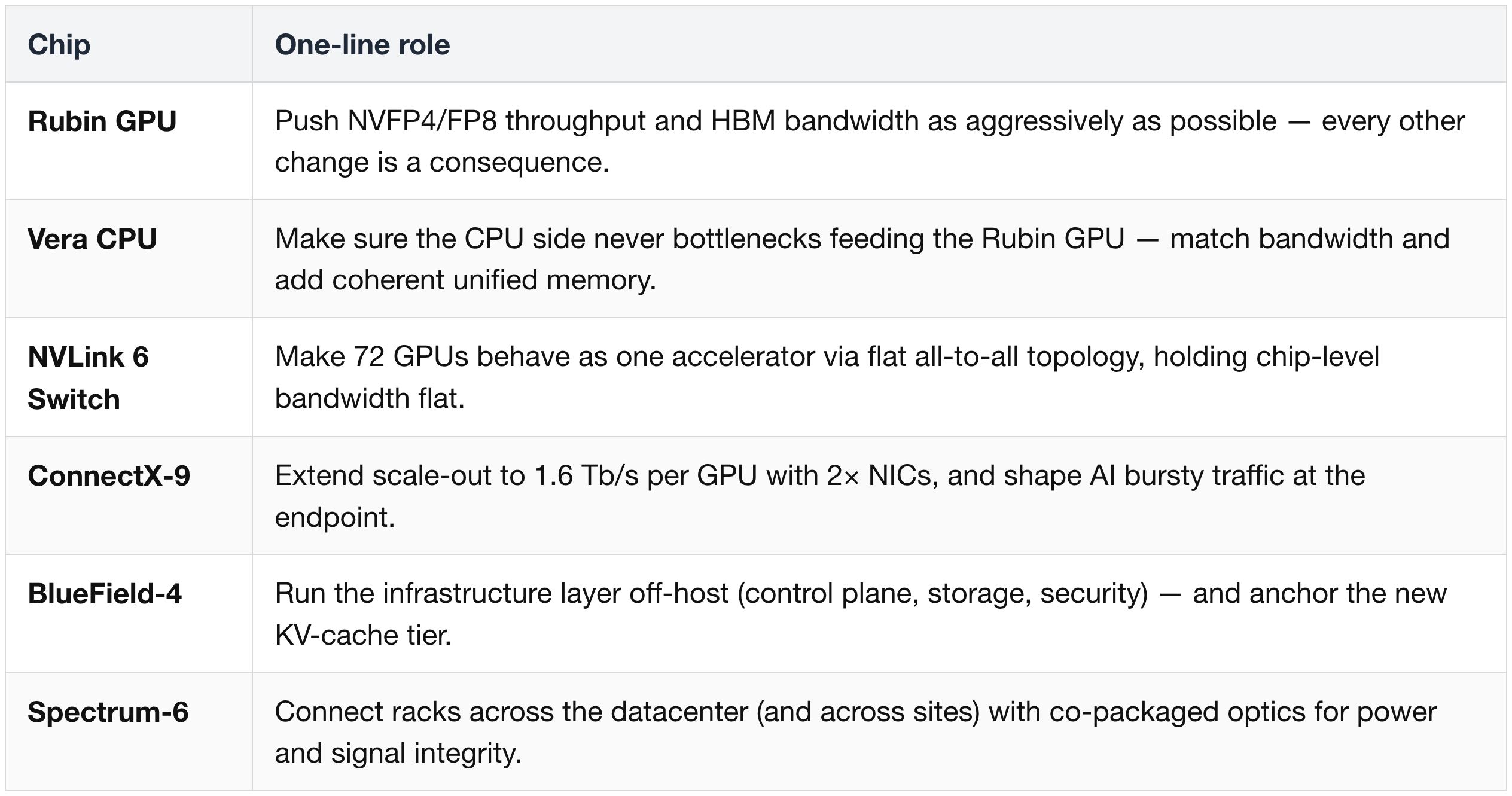
The whole VR NVL72 platform is the engineering consequence of two decisions: (1) treat the rack as the unit of compute, and (2) push every silicon component to the edge of what suppliers can build.
Where to Read What — Series Map
| Part | Title | Scope |
|---|---|---|
| 1 | Platform Framing & Architecture Map | Blackwell → Rubin platform thesis, headline specs |
| 2 | Rubin GPU — Engineering Deep Dive | Process node, SMs, HBM4, NVLink-C2C, package, CPX + Groq 3 LPX |
| 3 | Vera CPU & the Networking Silicon Family (this part) | Vera CPU, NVLink 6 Switch, ConnectX-9, BlueField-4, Spectrum-6 |
| 4 | Rack Assembly — Trays, PCB, and Cooling | HGX vs NVL72, compute tray modules, cableless midplane, PCB upgrade, liquid cooling |
| 5 | Rack Power and the Networking Fabric | Power delivery, HVDC, tray↔rack wiring, scale-up NVLink 6, scale-out InfiniBand + Ethernet |
| 6 | Supply Chain — Master Reference | Suppliers by subsystem across the entire stack |