Compute Was Never the Bottleneck — Moving Bits Is
The thesis in one breath
- Compute scaled ~60,000× in 20 years; the wires feeding it did not.
- The binding constraint on modern AI accelerators is moving bits — and it is one problem whether it happens between GPU↔GPU (the network) or GPU↔memory (the HBM bus), because both cross the same scarce die edge.
- Copper has run out of edge. Optics is the shared escape — but it arrives in phases; you cannot rip out SerDes for co-packaged optics overnight.
- Once optics is the I/O medium, memory stops being something you package next to the GPU and becomes something you connect to over the fabric — pools of compute and pools of cheap commodity DRAM on one low-latency optical fabric, routed by an optical switch.
- HBM doesn't die — it demotes to a cache tier.
How to read this note
- Section 0 — a refresher on why optics and why phased (kept tight).
- Sections 1–3 — the main argument: accelerators are network-bound → memory is part of the network → split the memory and connect it over an optical switch.
- Section 4 — who is building this, and where to focus.
Sources this note synthesizes
The argument is woven together from four sources without inline attribution. The direction is well-corroborated across all of them; the timelines and the magnitude of HBM's demise are the contestable parts, and each source carries its own slant.
- Irrational Analysis — HBM: High-Bandwidth Mistake (Jun 01 2026). The memory-disaggregation case. Opinionated and talking its book — long DRAM, explicitly pitching Samsung; the "90% HBM volume drop in 7–10 years" call rests entirely on the latency problem (§3) being solved at scale.
- SemiVision — Lightmatter Taiwan Tech Day in 20 Minutes (Jan 29 2026) and Lightmatter at Computex 2026: The Bottleneck Has Shifted from Compute to Interconnect (Jun 04 2026). The optical-fabric case; framing is Lightmatter-centric.
- SemiAnalysis — Co-Packaged Optics (CPO) Book — Scaling with Light. The CPO economics, phasing, and reliability data.
- Supplementary depth on the CPO transition, the DSP cost/power case, and Rubin's HBM4 pin-speed demand draws on the companion notes On CPO (Parts 1–2) and Vera Rubin Decoded (Part 2).
0 · Refresher — Why optics, and why a phased approach
0.1 The villain is the die edge ("shoreline")
What "shoreline" means
- A chip is an island: every external connection — power, memory, network — must cross its perimeter.
- That perimeter is fixed by die size, and the number of usable I/O lanes you can land on it is the shoreline (a.k.a. beachfront).
- As data movement intensifies, the coastline — not the core — becomes the bottleneck.
One wall, seen from two sides
- Both the AI networking story and the memory story reduce to the same sentence: the perimeter is a scarce resource and copper can no longer feed it.
- One framing calls it the shoreline problem; the other casts memory bandwidth as "an I/O density problem."
- They are describing one wall from two sides.
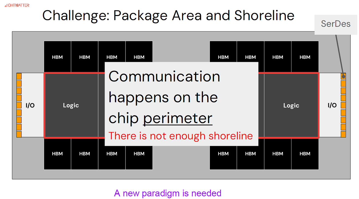
Logic surrounded by HBM, with SerDes I/O competing for the same edge. "A new paradigm is needed."
0.2 Copper's three walls
SerDes & PHY
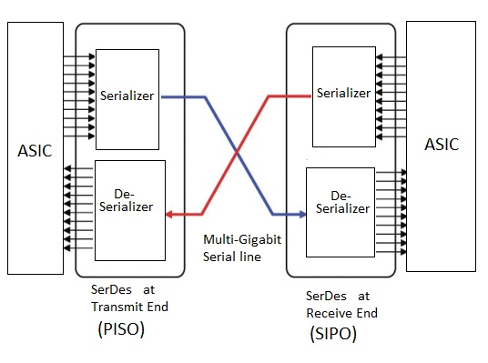
- SerDes (Serializer/Deserializer) drives a high-speed serial bit stream onto a copper lane and recovers it at the far end.
- PHY: The broader analog front-end that physically interfaces to the channel.
- Both live on the die edge and consume shoreline, power, and area.
The three walls, in order
- Reach. High-speed copper signalling dies after ~2 m. NVLink today delivers ~7.2 Tb/s per GPU over copper (Rubin targets ~14.4 Tb/s) — but only inside a single rack. You cannot scale a copper scale-up domain out indefinitely.
- Non-linear power. Per Broadcom, across recent switch generations bandwidth rose ~80× while system power rose ~22×, and SerDes/optics power has grown >3× faster than core logic. Power-per-bit gets worse exactly as you need more bits.
- Insertion loss at speed.
- Pushing a single copper lane to 224 Gbit/s (and "true" 448G) hits a signal-integrity wall: every bump, via, trace, and connector bleeds signal.
- PAM4 to 448G would need ~244 Gbaud — untenable on power and loss.
- Nvidia reaches 448G/channel only by bidirectional SerDes (224G Tx + 224G Rx sharing one channel), not true 448G unidirectional.
PAM4
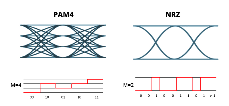
- Pulse Amplitude Modulation with 4 levels — encodes 2 bits per symbol (4 voltage levels) instead of 1, doubling bit rate for a given baud rate.
- Pushing further (PAM6/PAM8) buys bits but costs signal margin and power.
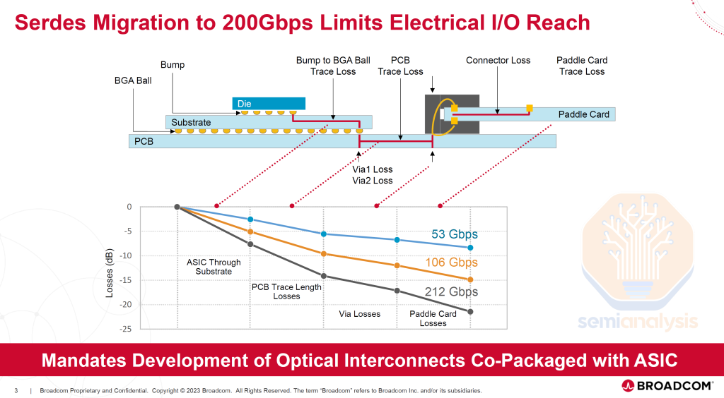
At 212 Gbps the channel loses ~20 dB before it even reaches the connector — "mandates development of optical interconnects co-packaged with the ASIC."
0.3 Why optics — and the figure of merit
Optics wins on the metric that matters: bandwidth density per unit energy, held across distance.
- Electrical links degrade exponentially with reach; optical links are nearly flat.
- The industry adage is "use copper where you can, optical when you must" — and the "must" line keeps moving toward the chip.
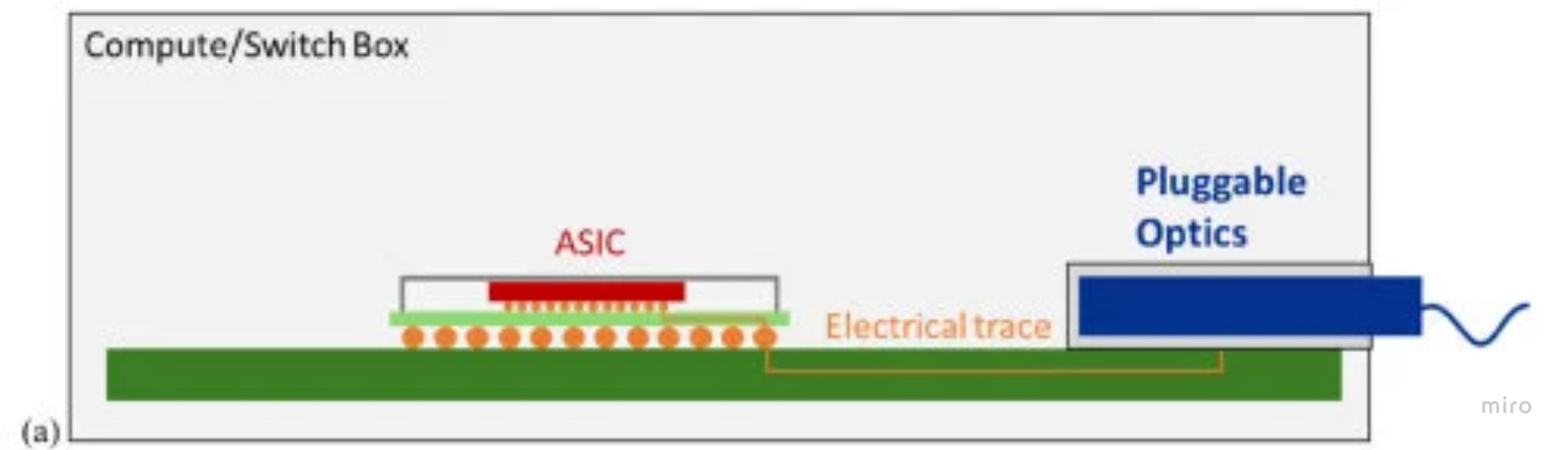
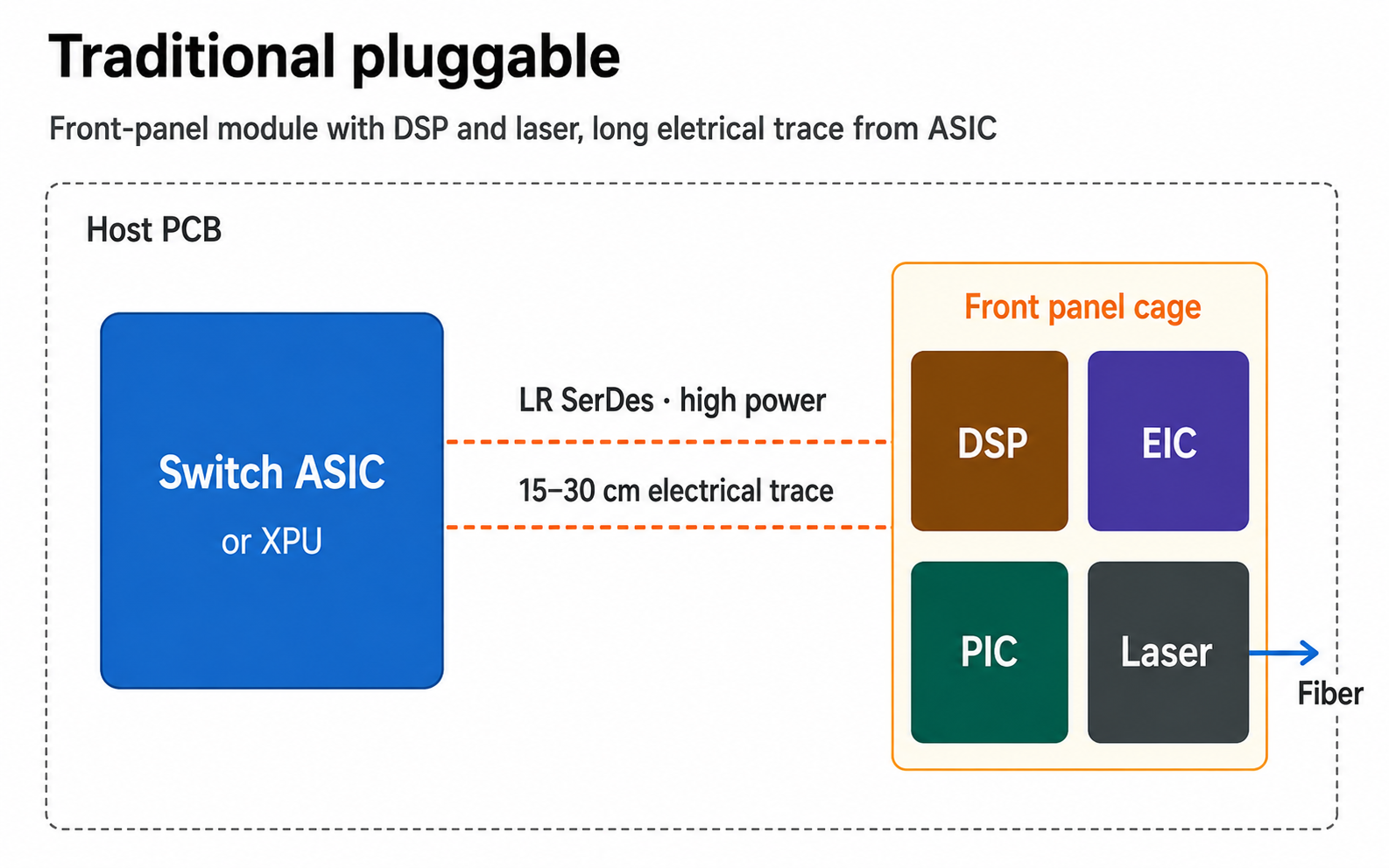
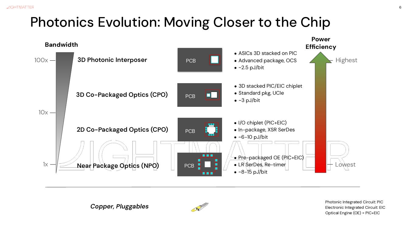
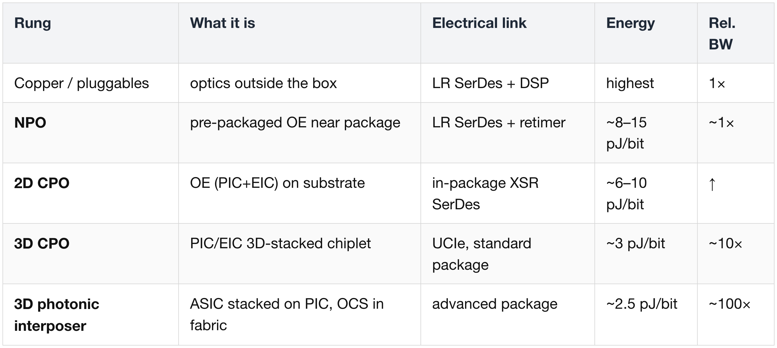
The proximity ladder: pluggables → CPO
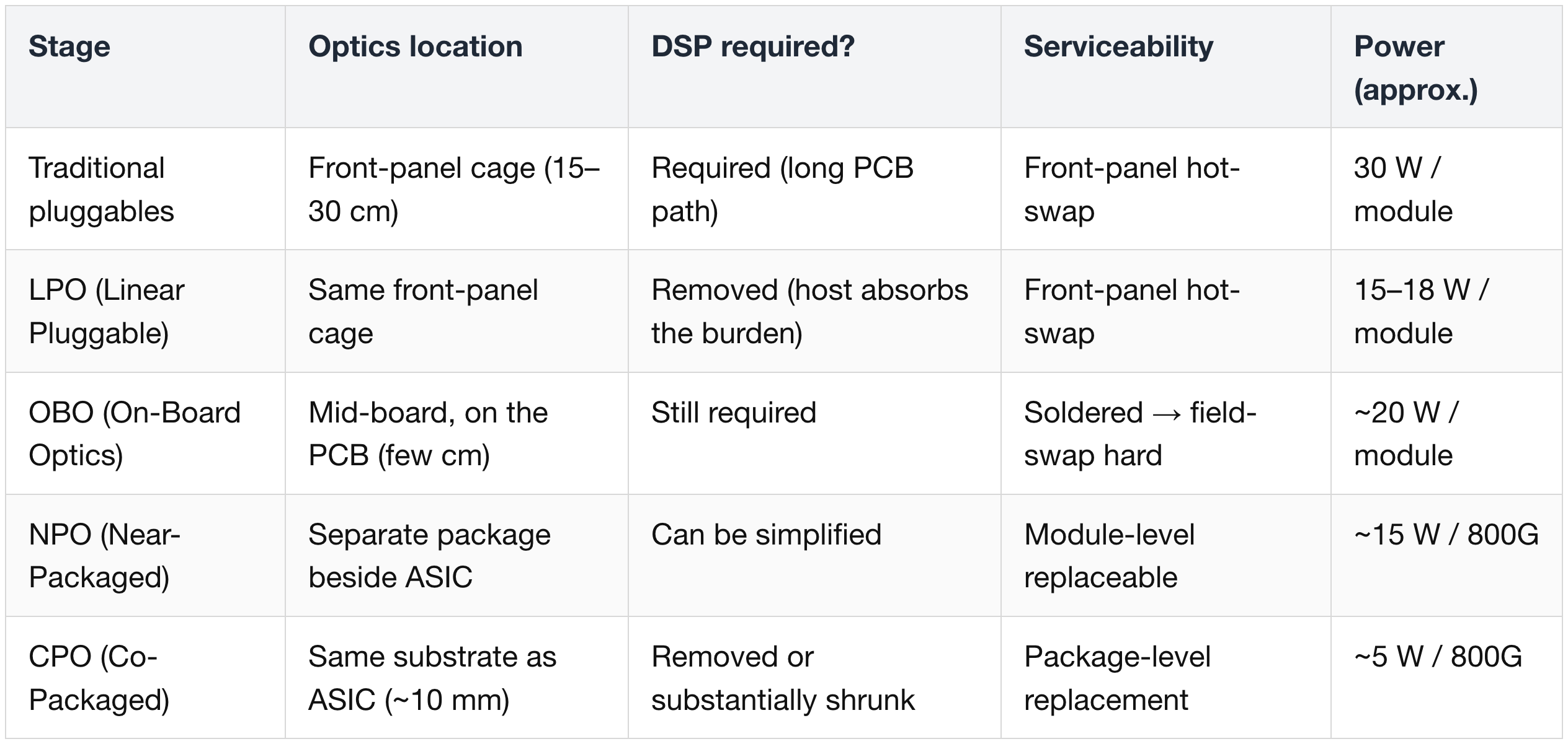
Optics moves toward the chip in stages; each rung shortens the electrical run before optical conversion, which is what lets you drop the DSP and shrink the SerDes. Power figures are per 800G.
- Traditional pluggables — engine in the front-panel cage (~15–30 cm). DSP required for the long PCB run. ~30 W; front-panel hot-swap.
- LPO (Linear Pluggable) — same cage, but the DSP is stripped and its burden pushed to the host. ~15–18 W. Orthogonal to the proximity axis — a pluggable variant, not a rung between OBO and CPO.
- OBO (On-Board Optics) — engine soldered mid-board (~few cm). DSP still required; soldered, so field-swap is hard. ~20 W. "Worst of both worlds" (CPO's complexity, pluggable's limits).
- NPO (Near-Packaged Optics) — engine near the package on a separate, often socketable substrate — still some copper to the SerDes; DSP can be simplified. ~15 W; module-level replaceable. An intermediate, lower-risk step.
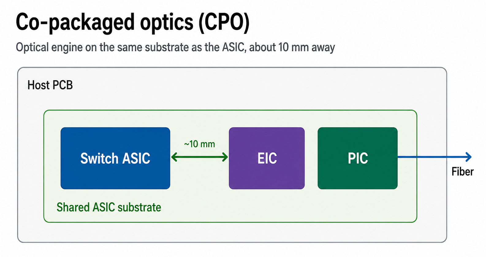
- CPO (Co-Packaged Optics) — engine on the host package (~10 mm). Kills the long-reach SerDes and the transceiver DSP. ~5 W; package-level replacement.
- OE (Optical Engine) = PIC (Photonic IC — modulators, waveguides, detectors) + EIC (Electronic IC — drivers, TIAs, control logic).
The same ladder, drawn as architecture cross-sections — the baseline, then each step pulling optics toward the ASIC:
Baseline — traditional pluggables: the module sits in the front-panel cage, 15–30 cm of lossy PCB from the ASIC. That long electrical run is exactly what the DSP exists to recover.
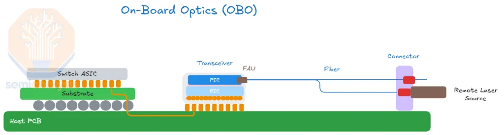
OBO: the module moves to mid-board near the ASIC, but the few-cm PCB run remains — so the DSP stays. Light reaches the front panel via an internal fiber jumper.
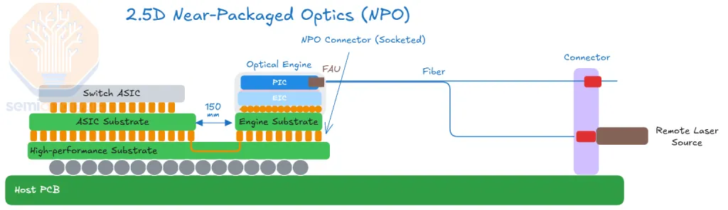
NPO: the optical engine sits beside the ASIC on the same PCB in a separate, replaceable package — a far shorter electrical run, and the DSP can be simplified.
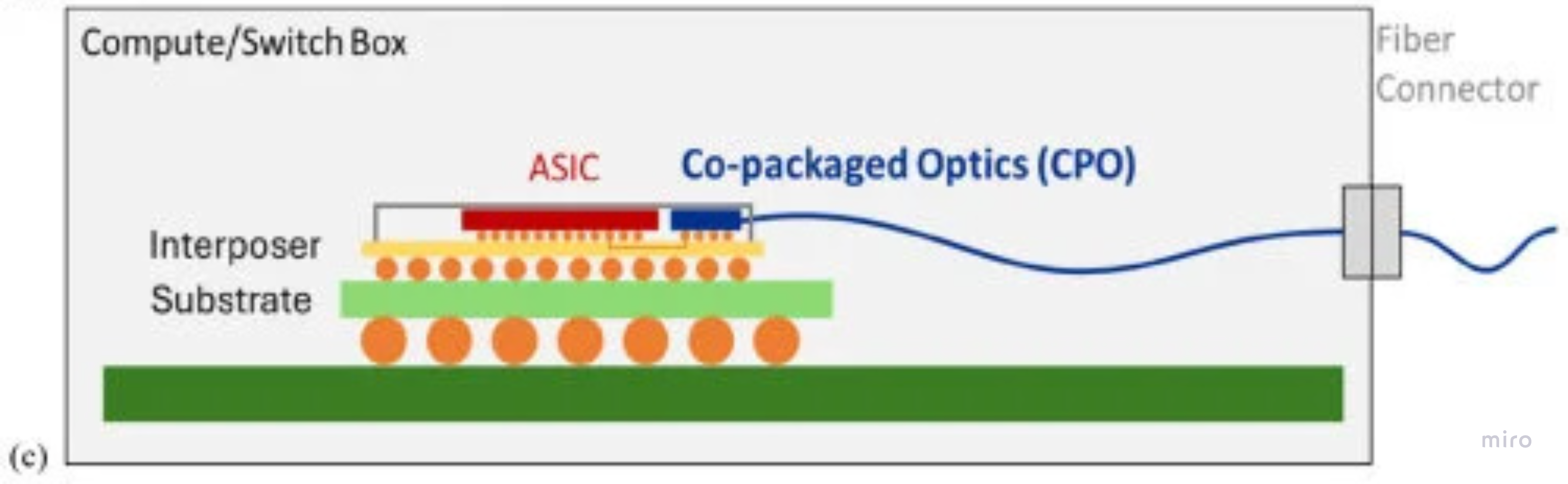
The three side by side — and only CPO lands the optical engine on the host substrate, collapsing the electrical path to ~mm and removing the DSP outright.
The DSP: public enemy on cost and power
- In a pluggable transceiver, the DSP retimes/reconditions the electrical signal degraded over the long copper run — it exists only to recover a signal that travelled too far.
- It is ~50% of an 800G module's power (~20 W of a 30 W module) and 20–30% of its bill of materials; transceivers themselves can be ~10% of cluster TCO. So the DSP alone is one of the largest single levers on both cost and power.
- Shorten the run via CPO and the DSP is no longer needed.
Worked example:
- An 18k-GPU GB300 cluster on a 2-layer InfiniBand fabric needs ~18,432 × 800G + ~27,648 × 1.6T transceivers;
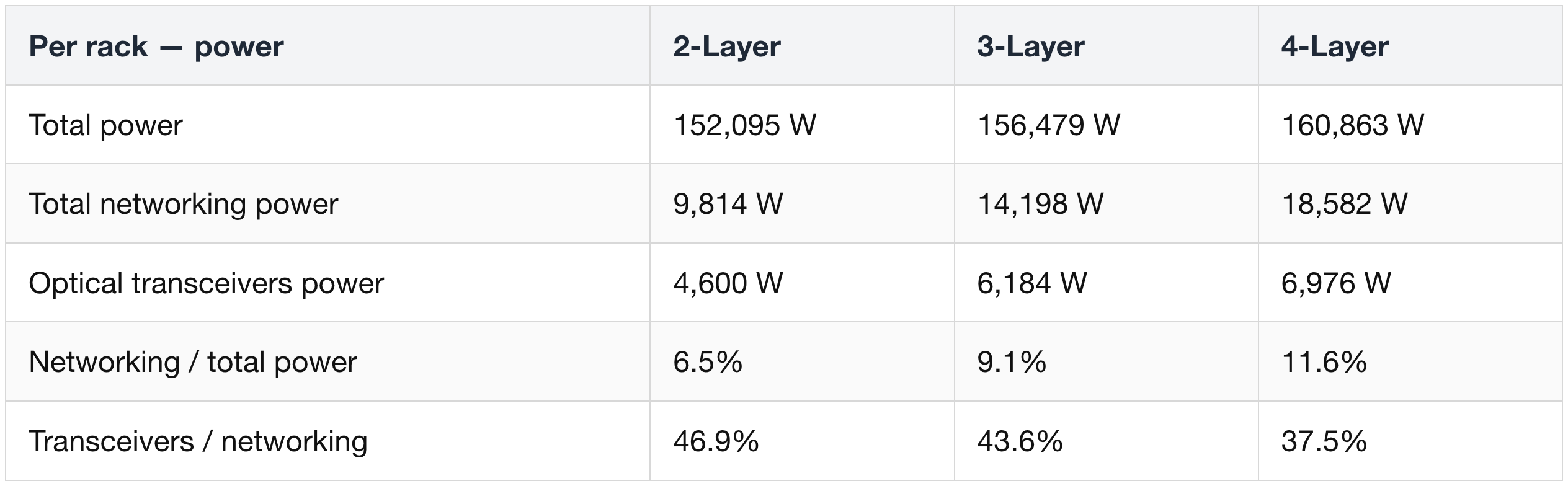
- budgeting 6–7 W (800G) and 12–14 W (1.6T) per DSP, that is ~480 kW of DSP power for the back-end network alone (~1.8 kW per rack). That is the prize.
DSP vs CPO — huge per-link, bounded at cluster scale
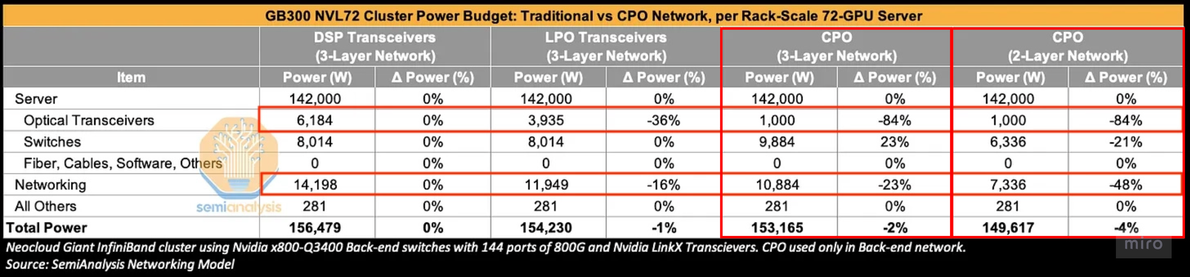
Swapping DSP transceivers for CPO: −84% transceiver power and −23% networking power net out to only ~2% of total cluster power. (3-Layer Network cluster basis)
Per link basis:
- The win is large, and two independent measurements agree. Compare a DSP-based pluggable against a CPO optical engine (OE) + external laser, normalized per 800G of bandwidth:
- 800G DR4 pluggable (from) ~16–17 W → (to) CPO OE + laser ~4–5 W = ~73% lower.
- 800G 2×FR4 pluggable (from) ~15 W → (to) OE + laser 5.4 W = ~65% lower. (Different module type, separate study — landing in the same ballpark is what makes the result credible.)
- Why the drop is so steep: the DSP is the bulk of a pluggable's power. CPO's short electrical run lets you delete it, and that single deletion is the largest contributor to CPO's headline ~50–80% per-link power saving.
Cluster scale basis:
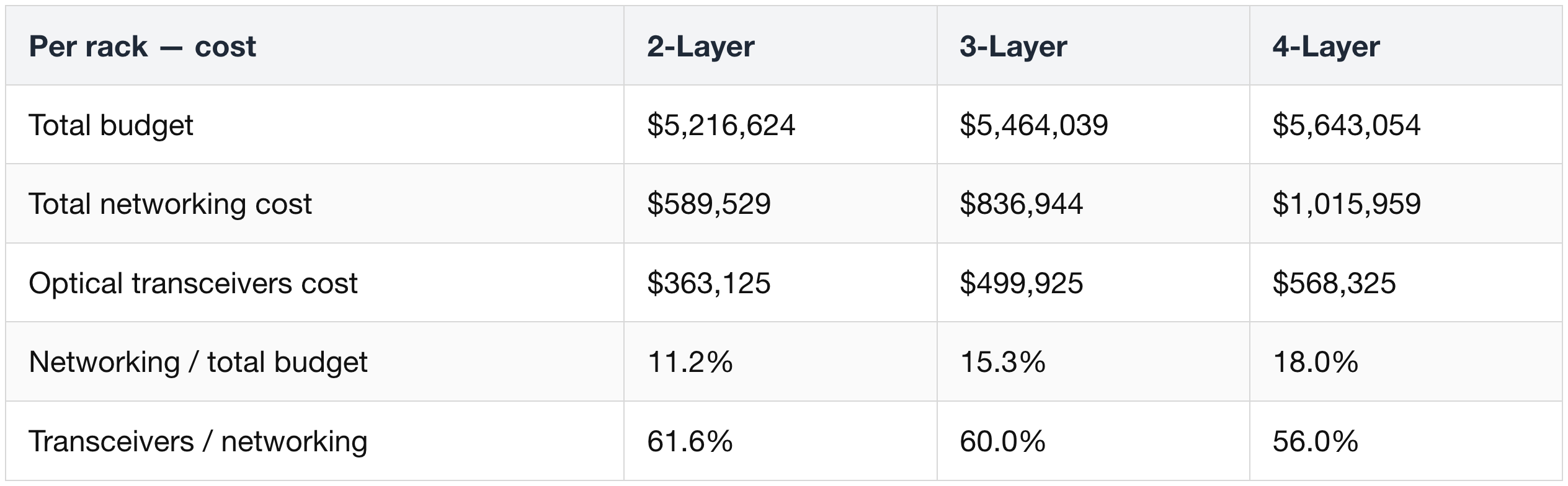
- At cluster scale it dilutes. Swapping DSP transceivers for CPO across a 3-layer GB300 NVL72 cluster cuts transceiver power ~84% and networking power ~23%.
- But networking is only ~9% of cluster power, so total cluster power falls only ~2% (≤~4% on a 2-layer net).
- Cost mirrors it: networking cost −21% but total cluster cost −3% (up to −46% / −7% on a 2-layer net).
- So the scale-out case is a capped power-saving story; the strategic pull is scale-up. A 2–4% power / 3–7% cost win can't, by itself, override serviceability, reliability, and vendor-lock-in fears.
- Where CPO becomes necessary rather than nice-to-have is scale-up, where copper/SerDes scaling hits a physical wall — which is exactly why the phasing runs scale-out → scale-up.
0.4 Why it must be phased
You cannot replace SerDes with CPO immediately. Optics climbs an integration ladder — each rung closer to the die, cheaper per bit, and harder to manufacture:
The phased path: copper/pluggables → NPO → 2D CPO → 3D CPO → 3D photonic interposer.
The gating factors are economics and operations, not physics
- Supply-chain immaturity.
- Reliability / yield.
- Serviceability — a failed soldered OE can brick a whole switch.
- Customers' fear of losing cost-control leverage — it is easier to squeeze many transceiver vendors than a few switch vendors.
What the reliability data actually says
- What the study showed — impressive on paper. Meta + Broadcom's ECOC study, run across a fleet of 15 × 51.2T switches (128 × 400G ports each), reported:
- a headline ~15M port-device hours logged in aggregate, with zero uncorrectable codewords observed up to ~4M of those hours;
- CPO MTBF (Mean Time Between Failures) ~2.6M hours vs ~0.5–1M for 2×FR4 pluggables.
- Why it's thinner than it looks. That 15M aggregate deflates fast once you divide it back out: 15 switches × 128 ports = 1,920 ports running in parallel, so 15M port-hours ÷ 1,920 ≈ 7,800 hours ≈ ~325 wall-clock days in a lab — a few months of runtime, not years of evidence.
- And a lab is not the field. Dust, thermal swings, thousands of switches — a different animal. Hence the conservative rollout: network optics first, slowly.
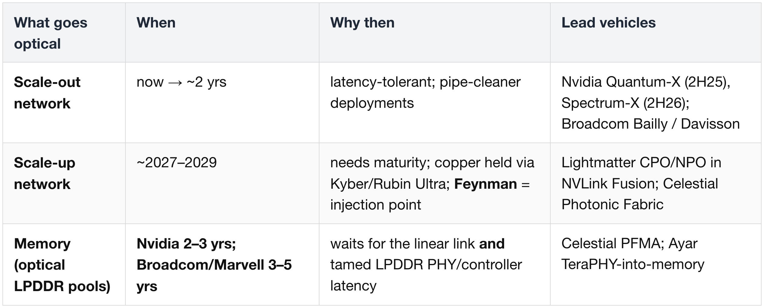
Phasing conclusion
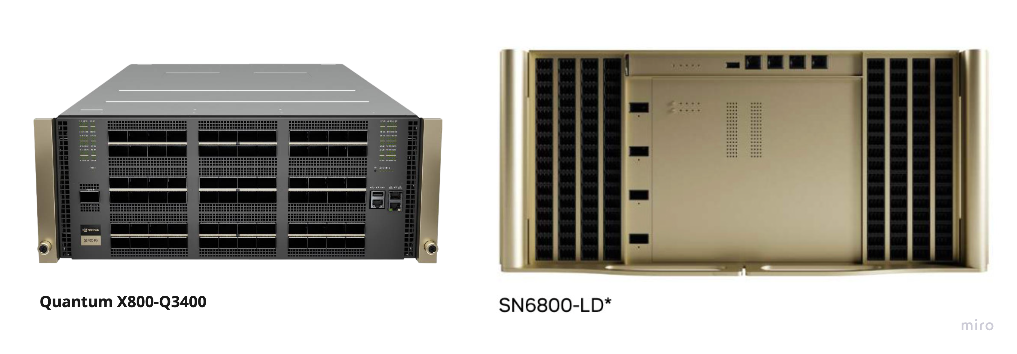
- Nvidia ships scale-out CPO switches first (Quantum-X in 2H 2025, Spectrum-X in 2H 2026) while holding scale-up on copper through the extreme Kyber / Rubin Ultra racks.
- The real high-volume CPO injection point looks like the Feynman generation.
- Latency-tolerant networking goes optical before latency-critical memory does (see §3.4).
1 · Moving bits matters: accelerators are network-bound
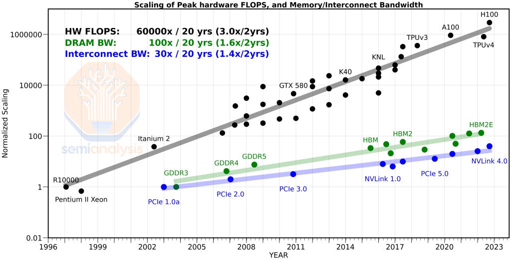
1.1 The chart that frames everything
FLOPS (top) vs DRAM and interconnect bandwidth (bottom). The compute line ran away from the feeding lines.
- Over ~20 years, peak hardware FLOPS scaled ~60,000× (≈3.0× every 2 years).
- DRAM bandwidth scaled ~100× (≈1.6×/2yr); interconnect bandwidth only ~30× (≈1.4×/2yr).
- Compute didn't just win — it lapped data movement by two to three orders of magnitude. That gap is the bottleneck.
The question stopped being "how fast is the GPU?" and became: can thousands — eventually tens of thousands — of XPUs behave like one giant distributed brain? The network is becoming the computer.
XPU
- Generic accelerator — a GPU or a custom ASIC (TPU, Trainium, MTIA, etc.).
- Used when the argument applies regardless of vendor.
1.2 World size, and the three expansion domains
Scale-up / scale-out / scale-across · world size
- Scale-up — tight, low-latency interconnect inside a rack/pod (~1 m).
- Scale-out — across racks/rows in a datacenter (~100 m).
- Scale-across — across datacenters / campuses (~10 km+).
- World size — the number of accelerators inside a single high-bandwidth (scale-up) domain. Bigger world size unlocks collective-communication tricks impossible across the slower scale-out network.
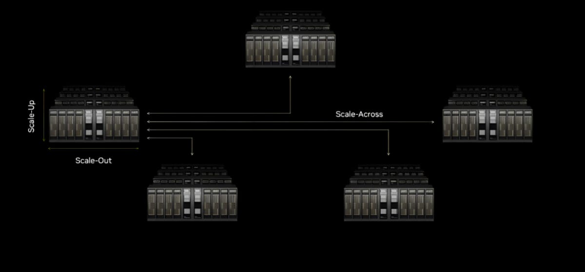
Three interconnect domains at three distance scales.
Two ways to grow world size — and copper's is brutal
GB200 jumped world size from 8 to 72 GPUs in one all-to-all domain — a huge throughput unlock. From there, the two paths diverge sharply:
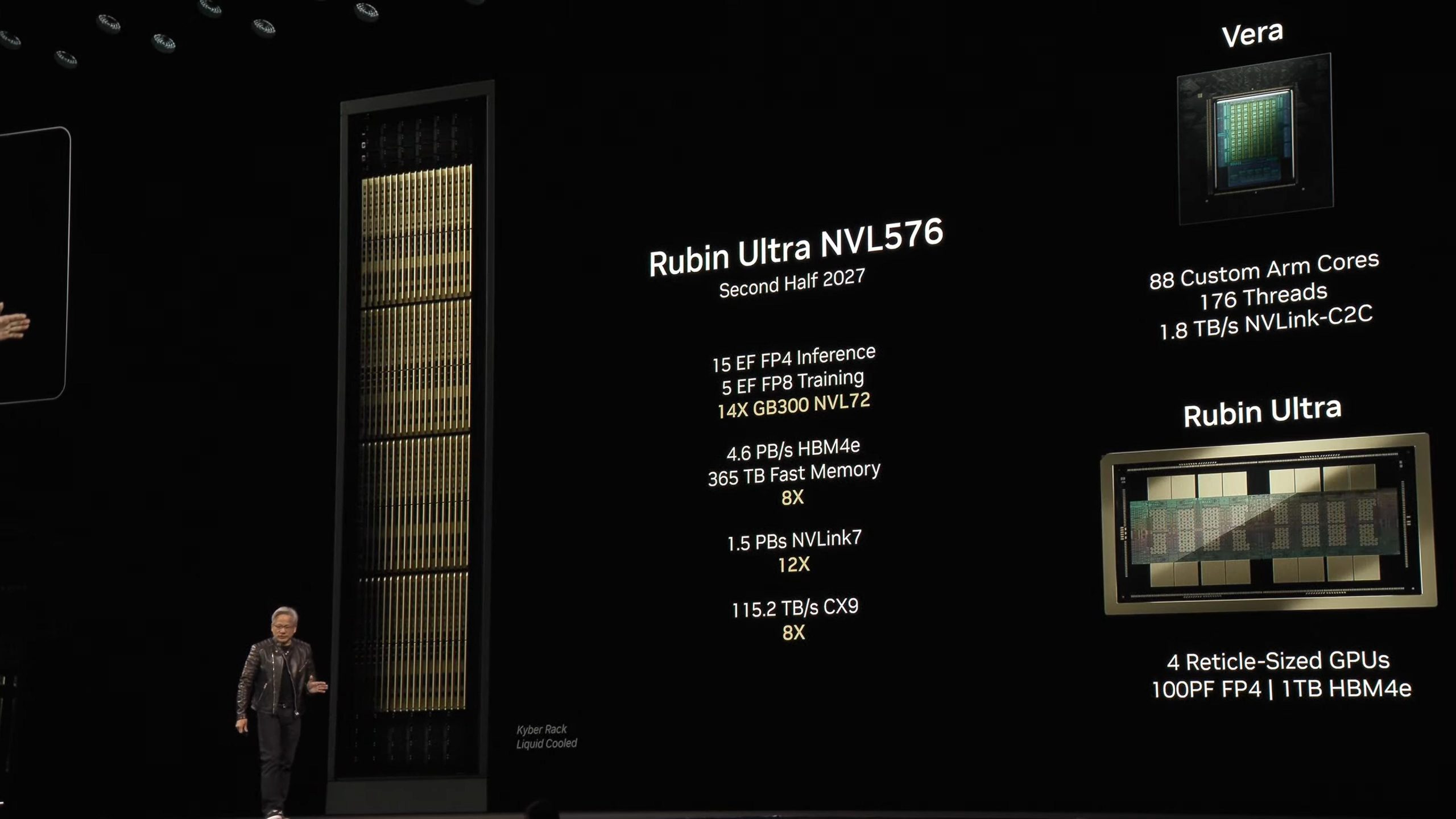
- Copper's path is brute densification. The upcoming (2H27) Kyber Rack scales to 144 GPU packages (576 GPU dies), ~4× denser than NVL72 — straining power delivery and thermals.
- Optics' path is the opposite escape: grow world size by reaching across racks instead of cramming a single one.
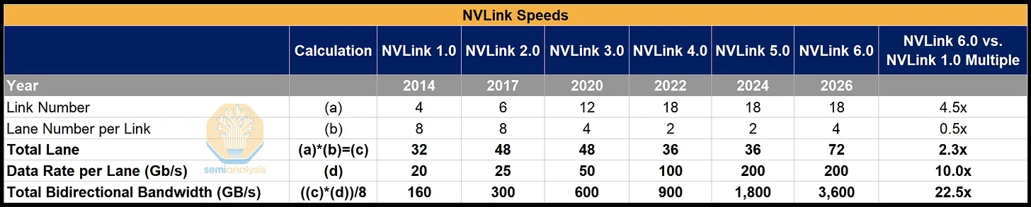
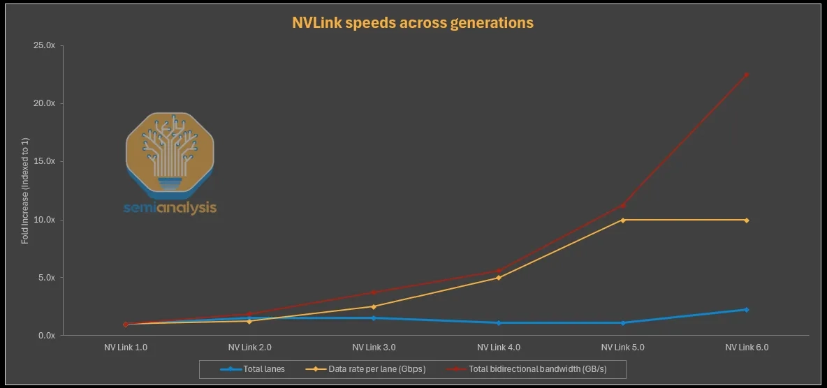
- NVLink's own history shows the copper squeeze.
- NVLink 5.0 has ~11× the bandwidth of 1.0, but lane count barely moved (32→36); the gains came almost entirely from a 10× SerDes speed-up (20G→200G).
- NVLink 6.0 stays at 200G and must double effective lanes via bidirectional SerDes — two signals on the same physical copper, no added shoreline. The plateau is visible.
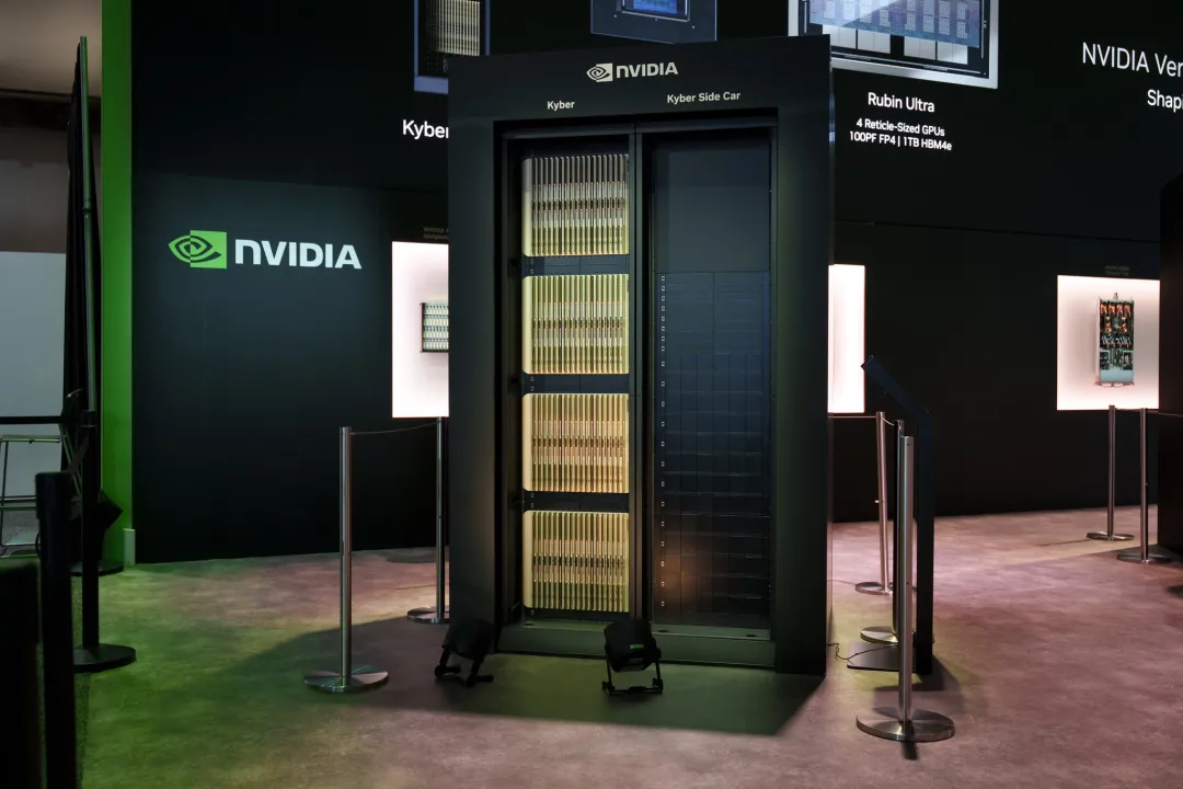
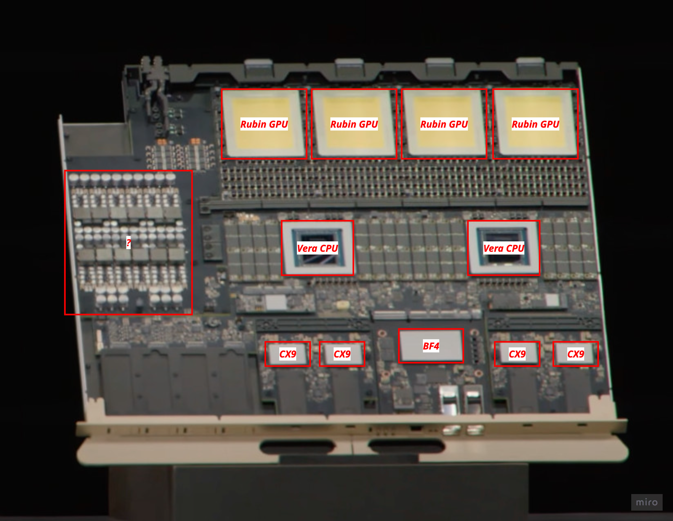
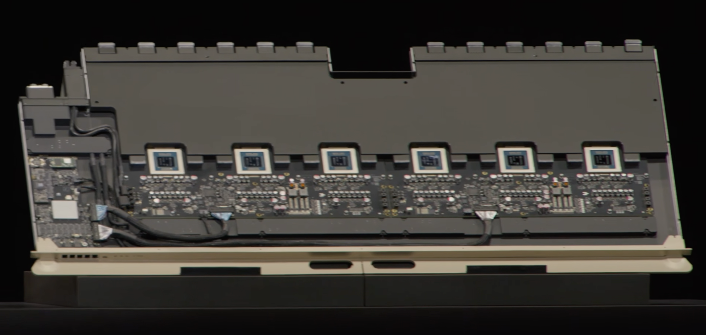
Btw this is how the Kyber Rack looks like:
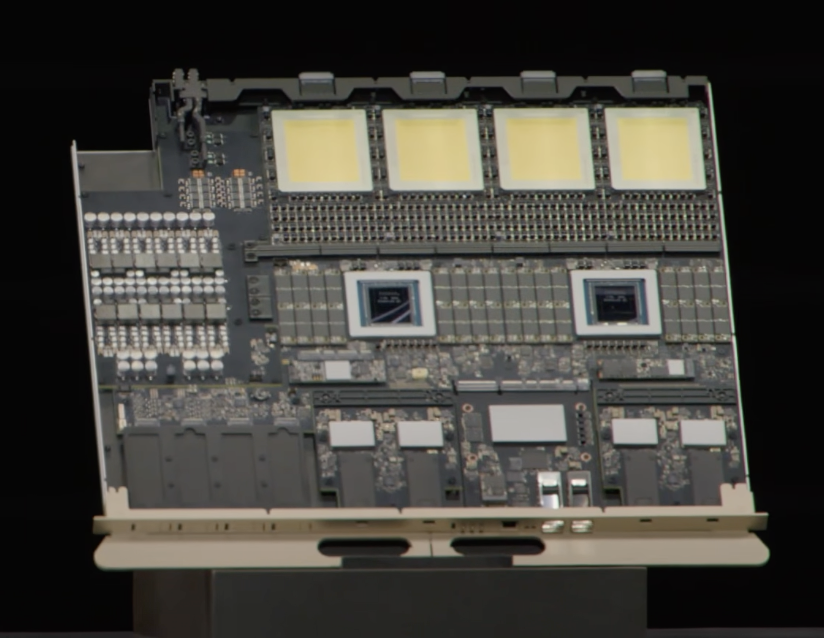
The individual compute blade (2 Vera CPUs, 4 Rubin GPUs):
The individual NVLink Switch blade:
1.3 Where the bottleneck bites hardest: decode
AI work splits into three regimes that stress infrastructure differently:
- Training — dominated by collective communication (synchronizing gradients across many devices). Compute-bound, but idle GPUs wait on the network.
- Prefill — dominated by time-to-first-token (TTFT). Compute-bound.
- Decode — latency-sensitive, memory-intensive, KV-cache-bound, and increasingly interconnect-limited as context grows.
KV cache · TTFT · MoE · radix
- KV cache — the stored keys/values of all prior tokens that decode must re-read each step; grows with context length and dominates memory traffic.
- TTFT — latency to the first output token (prefill quality-of-experience).
- MoE (Mixture-of-Experts) — scales parameters without activating them all per token, but routes tokens between experts/racks/memory pools, so the network determines real performance.
- Radix — a switch's port fan-out; higher radix = fewer hops = lower latency and fewer switch tiers, keeping MoE expert-parallel traffic inside the fast domain.
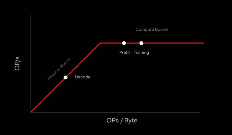
Roofline: decode lives in the memory-bound region; prefill/training are compute-bound.
The crux: memory movement and interconnect are the same problem
They meet in the decode / KV-cache regime.
- Lightmatter's Passage is positioned to cut training time ~3×, TTFT ~3×, and improve decode interactivity ~11× — the biggest win lands exactly where the bottleneck is worst (more on §4).
- "Memory is the new bottleneck" (memory demand could 5× in 5 years) is not a separate story from interconnect — it's the interconnect story applied to the KV cache.
2 · How we feed bandwidth today — HBM — and why it's a mistake
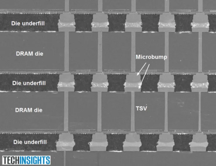
2.1 What HBM is
HBM · TSV · microbump · base die
- HBM (High-Bandwidth Memory) is DRAM stacked vertically.
- The dies are wired through TSVs (Through-Silicon Vias — vertical wires through the silicon) and joined by microbumps.
- The stack sits on a base die (a logic die with the PHY) and connects to the XPU through a silicon interposer.
- DRAM has only four knobs: latency, bandwidth, capacity, power. DDR / LPDDR / GDDR / HBM are the same cells in different arrangements — fundamentally interchangeable.
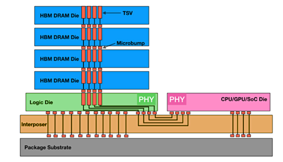
The HBM↔XPU channel runs PHY → interposer → PHY. The TSVs and that PHY are what consume shoreline.
High-level overview of components
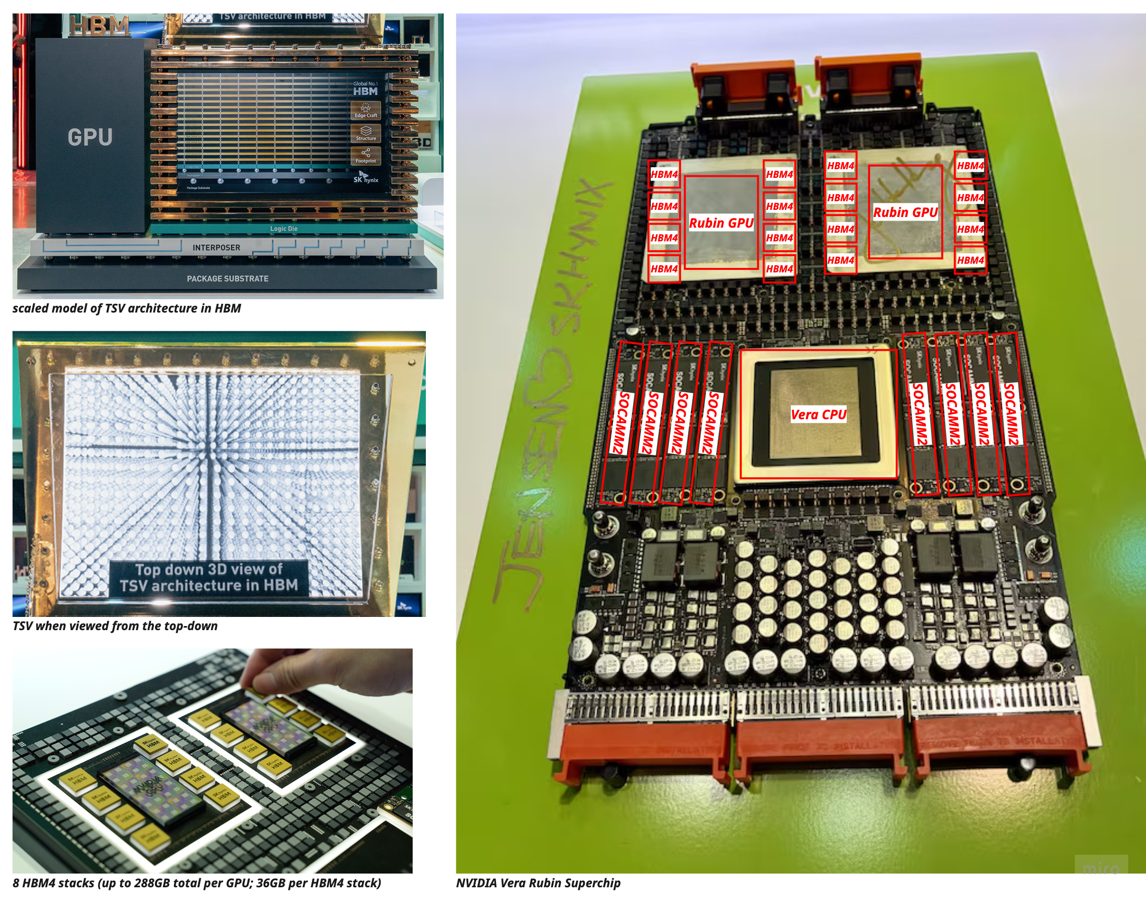
2.2 The HBM4 fiasco — a worked diagnosis
- JEDEC (the DRAM standards body) set HBM4 at 8 Gbps/pin; Nvidia's Rubin immediately demanded 11 Gbps/pin.
- All three vendors (SK Hynix, Samsung, Micron) initially struggled to meet it cleanly (all three have since qualified — see the update below).
- Root cause: bump capacitance.
Why Nvidia forced the issue
The above-spec demand wasn't gratuitous — it was competitive defence:
- Under the originally-announced 13 TB/s HBM4 target, AMD's MI450 would have shipped with higher memory bandwidth than Rubin.
- To stay ahead, Nvidia raised Rubin's target to ~22 TB/s (~2.75–2.8× Blackwell's 8 TB/s) at 288 GB — which is precisely what pushes pin speed past what JEDEC guarantees and forces all three vendors to validate parts above spec.
- The cost shows in the ramp: initial shipments likely land nearer ~20 TB/s until full pin speed qualifies — so above-spec pin speed is also a supply-continuity risk, not just an engineering one.
Update — GTC Taipei (2026-05-31): all three suppliers qualified
- Nvidia confirmed at the GTC Taipei keynote that Vera Rubin uses HBM4 from Micron, SK Hynix, and Samsung; by early June 2026 all three had qualified for Rubin production.
- Micron is in, but as a minority third source. Volume HBM4 shipments (36 GB 12-high, >11 Gbps) began in Q1 2026 — a quarter early — ramping ~2× faster than its HBM3E 12-high, on a 1-beta base die. (Early-April reports of base-die issues / sub-30% yields were resolved before qualification.)
- Allocation is lopsided: SK Hynix ~60–70% of HBM4 volume, Samsung ~25–30%, Micron the supplementary remainder. Micron's entire 2026 HBM supply is sold out under binding volume/price agreements struck in December 2025.
- For the thesis: the above-spec pin speed got met, not waived — which only sharpens §2.3's point that the structural shoreline/PHY tax, not raw pin speed, is the real ceiling.
Bump capacitance — why it kills speed
- Each microbump in the HBM stack adds a tiny parasitic capacitor.
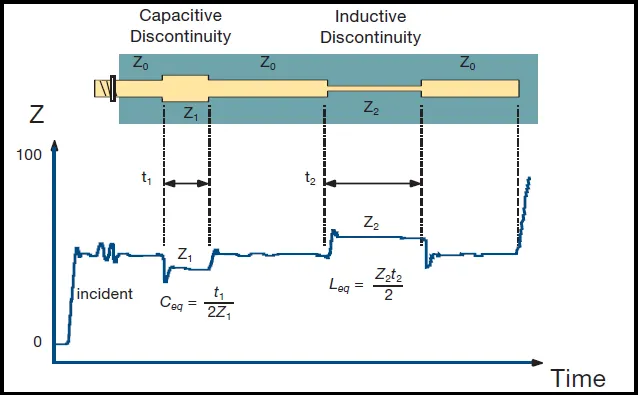
- On a TDR trace (time-domain reflectometry — an impedance "map" of the channel), a bare HBM stack shows one capacitive dip per layer.
- Capacitors act like speed bumps: at high frequency they distort the signal. You can perfect the base die, but the stack's parasitics still force you to either blow up PHY power or accept lower speed.
- The proper fix is hybrid bonding (direct copper-to-copper bonding, no solder microbumps) — and the key point is that speed, not just thermals or stack height, is what will finally force vendors onto it.
2.3 Why "HBM PHY is dogshit"
- 11 Gbps/pin is slow next to everything else on the package: 32G short-reach SerDes (UCIe-A, NVLink/Marvell/Broadcom D2D) are ubiquitous and 64G-class parts are shipping.
- The DRAM industry was handed a PHY problem and botched it.
- Custom HBM base dies (e.g. Marvell's cHBM) help — but only so much:
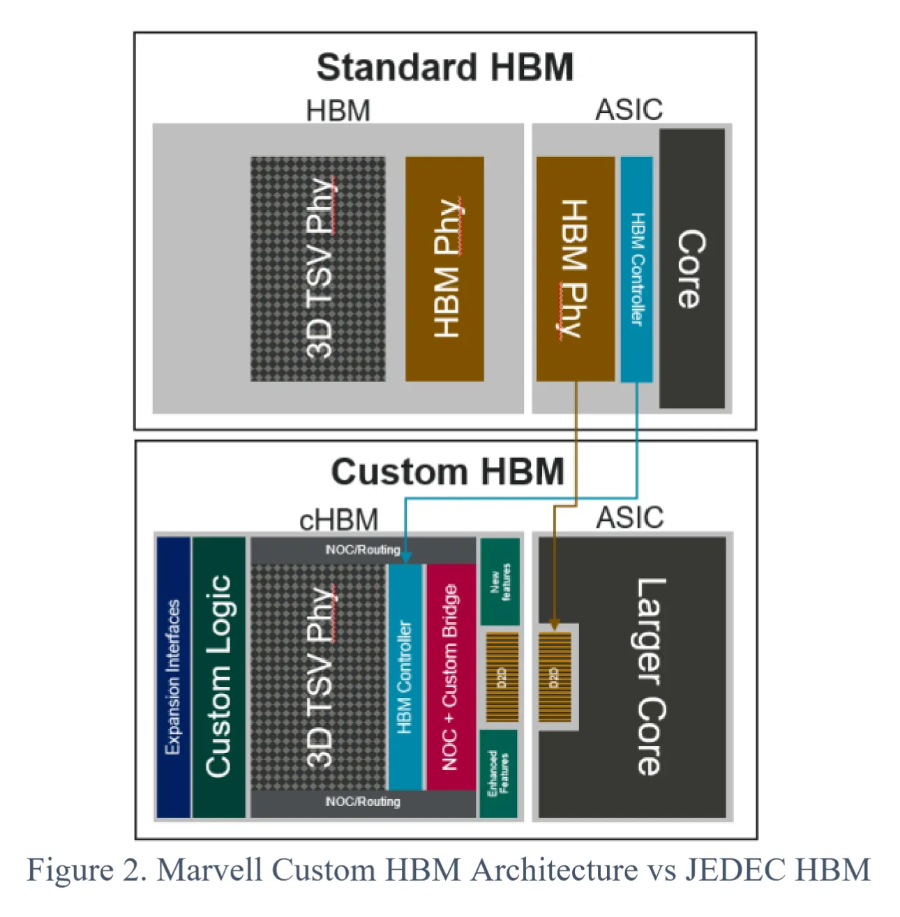
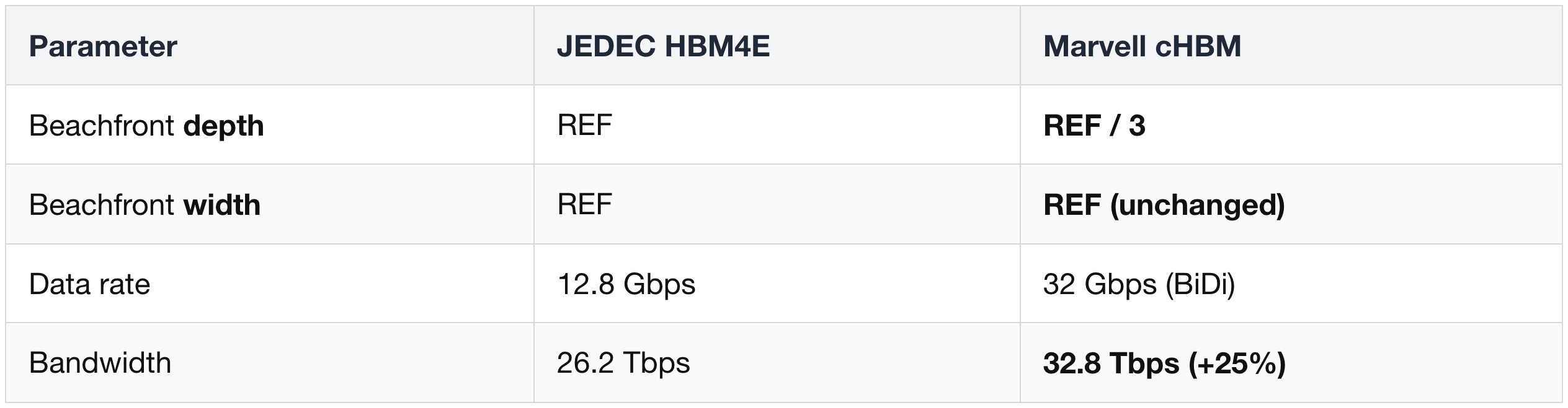
The tell is in the table:
- Beachfront width does not improve — because the TSVs still limit it. A better PHY buys ~25% bandwidth, but the structural shoreline tax remains.
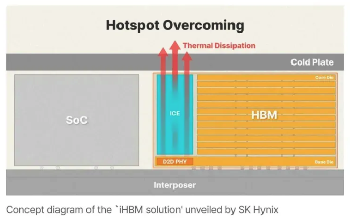
- SK Hynix's answer (iHBM) treats the symptom, not the cause.
- Hitting the pin speed means driving the PHY harder, which concentrates heat right at the D2D PHY — the hottest spot in the stack.
- SK Hynix's iHBM (announced May 2026) embeds thermally-conductive silicon Integrated Cooling Elements (ICEs) inside the package, directly at that PHY hotspot, adding a dedicated heat-dissipation path — ~30% lower thermal resistance. It is slated for HBM5 (~2029–2030), not HBM4.
- But it manages the heat rather than removing what creates it. The root-cause fix is hybrid bonding — kill the bump parasitics so you needn't over-drive the PHY in the first place. iHBM keeps the parasitic problem and bolts cooling on top: more silicon, more cost, more packaging complexity, to cool a self-inflicted hotspot.
- The underlying reason it never nets out: each gram of HBM bolted to the die steals shoreline, power, and thermal headroom from the logic at once. It is a zero-sum tax.
The spicy call
- HBM volume drops ~90% from peak within 7–10 years.
- A deliberately bold claim that rests entirely on the latency problem (§3) being solved at scale — flagged again in the caveats at the end.
2.4 CXL is only a partial fix
- CXL (Compute Express Link) — a memory-expansion / pooling protocol layered on PCIe.
- Useful (good for Marvell, Astera Labs), but it rides a sub-optimal PCIe PHY.
- We have a PHY problem; a protocol on top of the wrong PHY doesn't solve it.
3 · The better way: split the memory, connect it over an optical switch
3.1 The optimal future link (Nvidia, ISSCC 2026)
The endgame is clock-forwarded SerDes directly driving optics — glimpsed in Nvidia's ISSCC 2026 paper.
Clock-forwarding — why latency collapses
- Normally the receiver must recover the clock from the data, which requires a heavy equalization stack — CDR (clock/data recovery), FFE/DFE (feed-forward / decision-feedback equalizers), CTLE (continuous-time linear equalizer), MLSE (maximum-likelihood sequence estimation), plus a retimer and heavy FEC (forward error correction). All of that adds latency and power.
- Clock-forwarding sends the clock alongside the data, so the receiver can gut the entire EQ stack — "just a simple TIA" (transimpedance amplifier).
- This is the DSP-less / linear optical link — the only flavor fast and low-latency enough to serve memory.
The numbers (ISSCC 2026, clock-forwarded DWDM optical link)
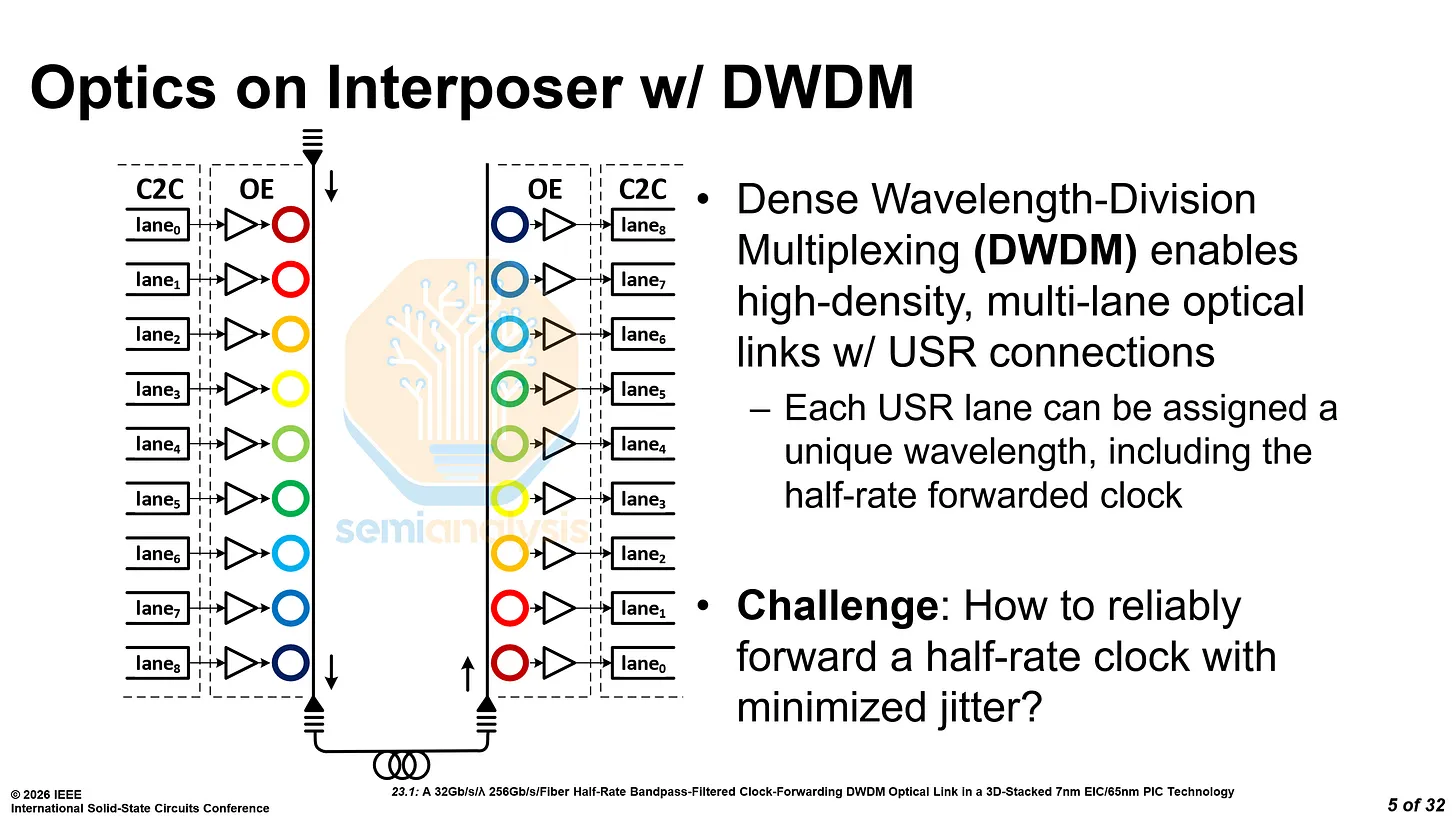
- 32 Gbit/s per wavelength × 9 wavelengths = 256 Gbit/s per fiber.
- EIC shoreline density ~0.8 Tbps/mm (bidirectional); BER < 1e-11.
- Total ~2.5–2.6 pJ/bit; reach 1–30 m.
- Caveat from the die shot: the Tx/Rx PLLs are as large as a whole lane — likely thermal-crosstalk isolation — so commercial shoreline density should improve well past today's ~0.4 Tbps/mm unidirectional.
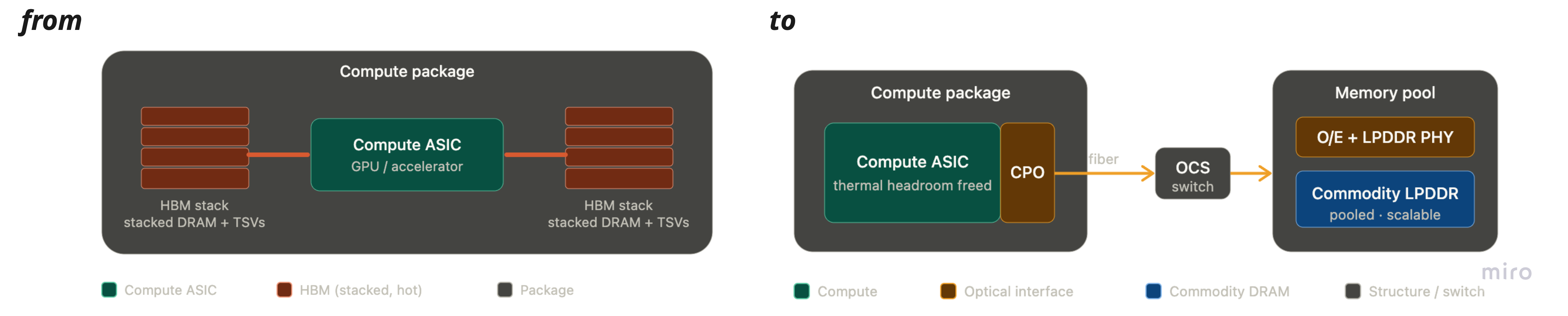
3.2 Route it with an optical switch — and memory becomes a network node

OCS (Optical Circuit Switch)
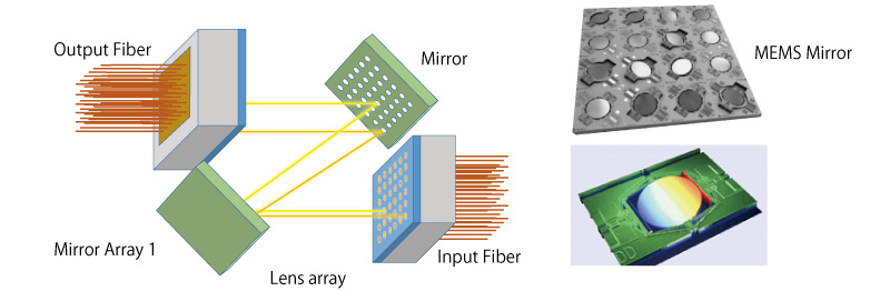
- A switch that redirects light paths directly (e.g. via MEMS mirrors) instead of converting to electrical, switching, and re-converting.
- It adds effectively no switching latency vs an electrical packet switch — which is what makes optically-attached memory viable.
The full picture — a four-step chain
- A clock-forwarded SerDes drives optics directly on the ASIC.
- An OCS routes the light with ~no added latency.
- At the far end a small chip converts optical→electrical and feeds LPDDR PHYs.
- Result — optically-attached, disaggregated LPDDR memory pools.
The load-bearing merge:
- Once optics is the I/O medium, "memory bus" and "network" stop being different things.
- Memory is no longer something you package next to the GPU; it's a resource you connect to over the fabric — architecturally indistinguishable from another node on the scale-up domain.
- Lightmatter's photonic interposer (with built-in OCS) is the natural home for exactly this.
3.3 The disaggregated AI factory — and why the win compounds
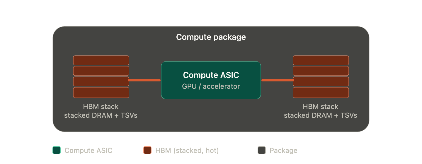
Merged: pools of compute + pools of cheap commodity LPDDR on one low-latency optical fabric, separately scalable. Removing HBM from the package unstacks a previously zero-sum problem all at once:
- frees shoreline — the TSV/PHY tax goes away;
- frees thermal budget — the ASIC can draw more power → more compute;
- the optical link replacing the copper memory bus is itself lower power-per-bit (~2.5–3 pJ/bit optical vs ~10 pJ/bit for a 224G copper link counting both ends — roughly 3–4× better at the link level).
HBM doesn't vanish — it demotes to cache
- The realistic terminus is a tiered memory system: a small, fast local HBM/SRAM cache for the hottest data, backed by a big optically-attached LPDDR pool.
- In the optical end state, "perhaps a stack of HBM somewhere used as a cache will be needed" — latency there is dominated by the LPDDR PHY and controller, not the optics.
3.4 Why memory optics lags network optics
One gate unifies the phasing: latency
- Networking tolerates some latency; memory does not.
- Network-side optics ships first (CPO/NPO now → ~2 yrs; Lightmatter is already in the NVLink Fusion ecosystem).
- Memory-side optics follows only once (a) the clock-forwarded / linear optical link matures and (b) the LPDDR-side PHY/controller latency is tamed.
- The winning link on both cases is the ultra-low-latency, DSP-less, linear kind — the "Optical I/O / Near-DSP" branch, not heavy-DSP coherent optics.
3.5 The economics mirror the engineering
The "everyone wins" math
- HBM trade ratio ≈ 3:1 — producing 1 GB of HBM consumes ~3 GB of commodity DRAM capacity (the stacking/yield overhead). So shifting from HBM to LPDDR roughly triples usable DRAM bit supply.
- Now the profit pool. Today HBM runs ~80% gross margin. Picture an LPDDR world: 3× volume, margin down to ~60%.
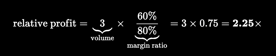
- Vendors make ~2.25× profit on 3× revenue at a softer margin.
- Customers escape ~80%-margin pricing and advanced-packaging yield risk, and reclaim package area for logic.
- Unbundling memory from the ASIC unbundles the DRAM industry's pricing power. (Whether the exact ratios hold is debatable; the structural claim is the financial shadow of the technical one.)
4 · Industry adoption & companies to focus on
The meta-rule: co-design depth wins
- Whoever owns the whole channel optimizes it best.
- NVLink leads because Nvidia (NASDAQ: NVDA) controls package, PCB, SerDes, and cables end-to-end ("Ethernet without the generalization or interoperability") — if you know the channel ahead of time, you tune the SerDes for that channel.
- The same logic elevates foundries from "manufacturing service" to opto-electronic platform providers — e.g. TSMC (TPE: 2330) with COUPE — and, on the memory side, favors the one DRAM vendor that can co-design across electrical and optical.
4.1 The optical-fabric & optical-memory builders
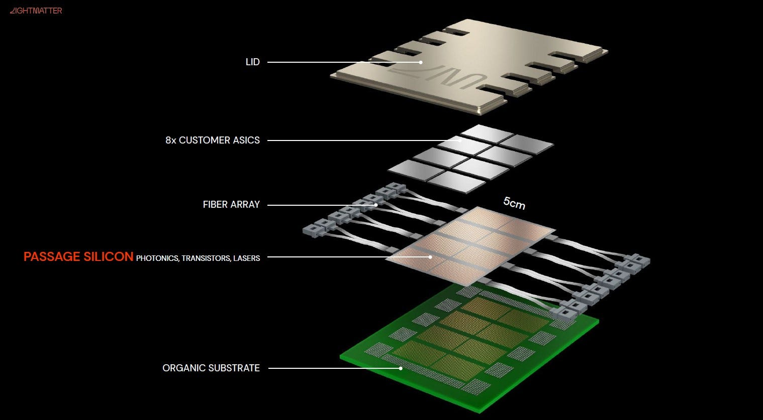
Lightmatter (private) — the photonic-interposer bet
Passage is not a module; it's a photonic interposer that pulls optics into the package fabric, with built-in optical circuit switching.
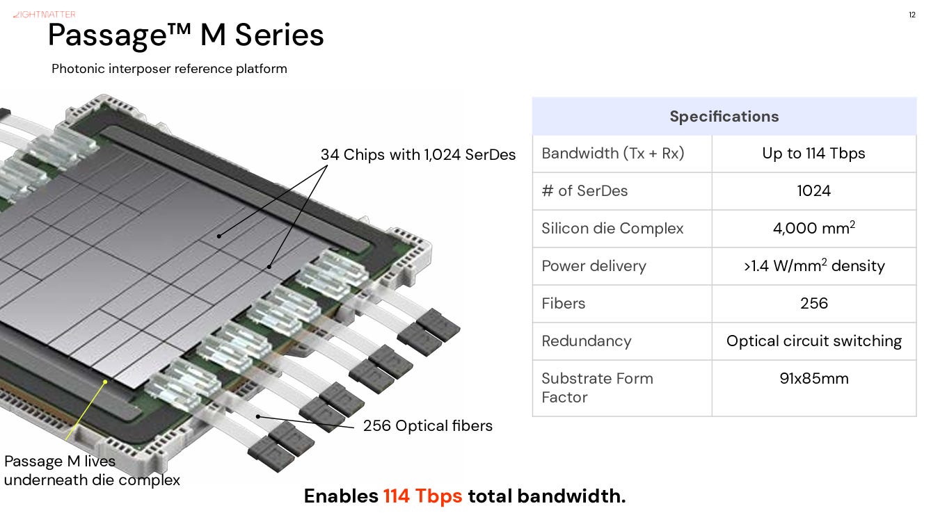
Passage M1000: a 4,000 mm² optical interposer beneath the compute dies, 114 Tbps via 1,024 low-power (~8× smaller) SerDes at 112 Gbit/s each, with OCS in-fabric.
- Roadmap: NPO (L20) in 2026/27 → CPO in 2027/28 → flagship M1000 interposer in 2029+, aligned to TSMC COUPE.
- Owns its laser (Guide — a Very-Large-Scale-Photonics source integrating hundreds of InP lasers per chip, up to ~50 Tbps; two Guides can feed a Quantum-X switch that otherwise needs 18 external laser sources).
- Solves serviceability with eClick/vClick detachable fiber-array units (<1.5 dB insertion loss), and fiber economy with BiDi + DWDM.
- Now an optics partner in the NVLink Fusion ecosystem.
Celestial AI (private; acquired by Marvell) — the optical-memory company
Its Photonic Fabric puts modulators/detectors/waveguides into the interposer and places optical I/O in the center of the die, freeing the perimeter. The flagship for this thesis is the Photonic Fabric Memory Appliance (PFMA) — an in-network shared memory pool.
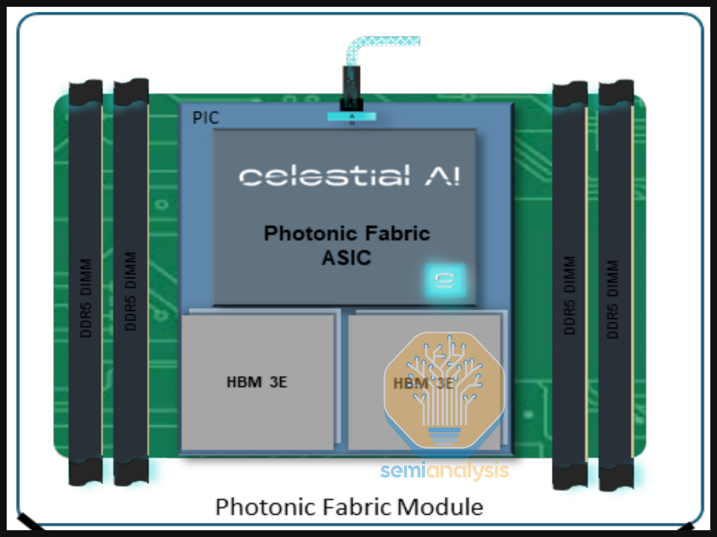
Memory as a networked resource: HBM3E + DDR5 behind a Photonic Fabric ASIC, reached over fiber — a "warm" KV-cache tier between HBM and storage.
- PF chiplet 16 Tbps → 64 Tbps (gen 2).
- Uses EAM modulators — far better thermal tolerance than MRMs, which matters when the modulator sits under a hot XPU.
- ~2.5 pJ/bit for the whole E-O-E link (+~0.7 laser) vs ~10 pJ/bit for copper.
- Acquired by Marvell, with warrants pointing at AWS (Amazon, NASDAQ: AMZN) Trainium 4 as the volume target (~late 2027).
Ayar Labs (private) — the standards-friendly optical chiplet
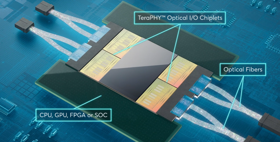
- TeraPHY is a UCIe optical chiplet that can be packaged into an XPU, a switch, or memory — directly enabling the optical-memory endpoint.
- Roadmap 4 Tbps → ~13.5 Tbps per OE (8 OEs ≈ ~108 Tbps per package, with Alchip (TPE: 3661) / GUC (TPE: 3443)).
- Backers include Nvidia, AMD (NASDAQ: AMD), TSMC, Intel (NASDAQ: INTC), GlobalFoundries (NASDAQ: GFS) — a who's-who hedging the bet.
4.2 The incumbents who own the channel
Nvidia
- Ships scale-out CPO first (Quantum-X 115.2T 2H25; Spectrum-X 102.4T/409.6T 2H26), holds scale-up on copper through Kyber, and authored the clock-forwarded optics ISSCC paper.
- ~2–3 years from optical memory at scale.
- Controls the whole channel — the structural reason NVLink leads.
Broadcom (NASDAQ: AVGO)
- The most CPO-experienced switch vendor (Humboldt → Bailly 51.2T → Davisson/TH6 102.4T), now an OpenAI (private) ASIC partner and migrating to TSMC COUPE (grating coupling + MRMs — a partial reset).
- ~3–5 years for memory optics.
- Has shown experimental packages co-locating an OE with logic + HBM.
Marvell (NASDAQ: MRVL)
- Custom cHBM base dies, CXL, D2D IP — and now owns Celestial AI, buying its way into optical memory.
- ~3–5 years.
Samsung (KRX: 005930) — the memory-side pick
The cleanest pure-play on "split the memory":
- The only DRAM maker with an in-house logic foundry + interface IP + a SiPho/CPO group, so it can co-design "across electrical and optical" — HBM PHY, TSV PHY, DRAM, interface IP, and the optical link together.
- On that stack, Samsung Foundry SiPho rates ahead of GlobalFoundries and its CPO group ahead of AMD's.
- This is the memory-vendor version of the co-design thesis: the one DRAM vendor positioned to own both the electrical and optical sides of the channel.
4.3 Supporting cast
- TSMC — COUPE is becoming the default OE integration platform (hybrid-bonds PIC on mature N65 + EIC on N6); biases the ecosystem toward grating coupling + MRMs. The platform almost everyone routes through.
- Positron (private) — the standout startup here; an AI ASIC using only commodity LPDDR5X (no HBM) with the highest memory bandwidth of any ASIC. The "correct" short-term answer before optics matures.
- Xscape (private) (programmable 4–128-wavelength laser, one fiber), Nubis (private) (single-wavelength, dense 2D fiber arrays; acquired by Ciena, NYSE: CIEN), Scintil (private) (wafer-level III-V-on-silicon DWDM lasers), Ranovus (private) (interoperable Ethernet-standard CPO with MediaTek (TPE: 2454) / AMD). Laser sourcing itself becomes an infrastructure layer.
4.4 Where to point attention
- Pure thesis play (memory): Samsung (electrical+optical co-design), Celestial AI / Marvell (in-network optical memory), Ayar Labs (memory-capable optical chiplet).
- Optical fabric: Lightmatter (photonic interposer + OCS, NVLink-Fusion partner).
- Channel owners / timing-setters: Nvidia (sets the phasing; 2–3 yr to optical memory), Broadcom (3–5 yr).
- Platform / enabler: TSMC (COUPE). Short-term bridge: Positron (LPDDR-only, no HBM).
Unified thesis
- Compute was never the bottleneck — moving bits is.
- Moving bits spans GPU↔GPU and GPU↔memory because they are the same die-edge I/O wall.
- Optics is the shared escape, and once it's the I/O medium, memory dissolves into the network — a disaggregated factory of compute pools and cheap LPDDR pools on one low-latency optical fabric.
- The network gets optics first; memory follows once the DSP-less, clock-forwarded link is cheap and fast enough.
- HBM ends as a shrinking cache tier, not the main store.
Caveats (the sources are opinionated and forward-looking)
- The underlying sources each carry a slant — one is long DRAM and pitching Samsung; another frames everything around a single optical-fabric vendor (see the Sources block up top).
- The "90% HBM volume drop in 7–10 years" rests on the latency problem actually being solved at scale.
- The direction is well-corroborated; the timelines and the magnitude of HBM's demise are the contestable parts.