On CPO Pt. 2 | The Economic and Architectural Case for CPO

Why scale-out's cluster-level TCO impact gets diluted, why scale-up forces Nvidia to adopt CPO to defend its NVLink moat, and the mechanism by which the bottleneck migrates to packaging.
On CPO
- Part 1, The Phased Transition from Pluggables to CPO
- Part 2, The Economic and Architectural Case for CPO
- Part 3, Inside the Optical Engine
- Part 4, Today's Major CPO Products
- Part 5, OCS, Testing, and the Optical Value Chain
2. Scale-out: TCO Savings are Real, but Diluted
AI cluster networking generally splits into three fabrics.
| Fabric | Role | Typical bandwidth / character |
|---|---|---|
| Front-end fabric | Connects the AI cluster to users, applications, storage, and external networks; primarily handles ingress / egress, data loading, and service (north-south) traffic. | 100G / 200G |
| Back-end fabric | Handles GPU-to-GPU / XPU-to-XPU connectivity, carrying the high-bandwidth, low-latency east-west compute traffic of distributed training and inference. | 400G / 800G, high bandwidth, low latency, typically lossless |
| Out-of-band management | A network dedicated to hardware management. | Low bandwidth, high availability, isolated. |
From a CPO standpoint, the back-end network matters most.
- It is technically the most demanding fabric.
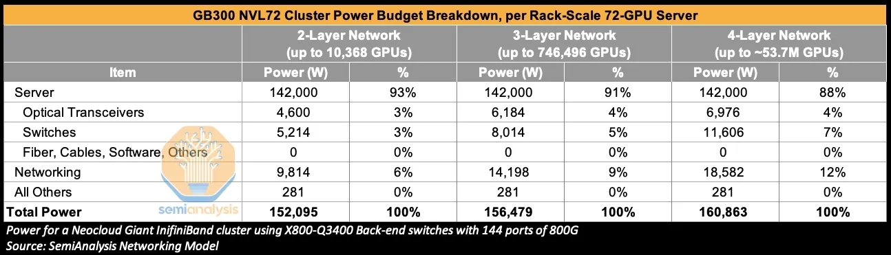
- In the source model, the back-end network accounts for 85% of networking cost and 86% of networking power for a 3-layer GB300 NVL72 cluster.
(1) Networking is the second-largest line item in AI cluster build-out cost (after the AI server)
And more than half of that line item is the cost of pluggable transceiver modules.
The more GPUs in the cluster, the more networking layers you need. Going from a 2-layer to a 3-layer or higher network (i.e. as scale-out demand rises) drives both cost and power budgets up.
Per-rack cost basis for a GB300 NVL72:
| 2-Layer Network | 3-Layer Network | 4-Layer Network | |
|---|---|---|---|
| Total Budget | $5,216,624 | $5,464,039 | $5,643,054 |
| Server cost | $4,357,943 | $4,357,943 | $4,357,943 |
| Total Networking cost | $589,529 | $836,944 | $1,015,959 |
| Optical Transceivers cost | $363,125 | $499,925 | $568,325 |
| Total Networking / Total Budget | 11.2% | 15.3% | 18.0% |
| Optical Transceivers / Total Networking | 61.6% | 60.0% | 56.0% |
Per-rack compute power demand basis for a GB300 NVL72:
| 2-Layer Network | 3-Layer Network | 4-Layer Network | |
|---|---|---|---|
| Total Power | 152,095W | 156,479W | 160,863W |
| Server power | 142,000W | 142,000W | 142,000W |
| Total Networking power | 9,814W | 14,198W | 18,582W |
| Optical Transceivers power | 4,600W | 6,184W | 6,976W |
| Total Networking / Total Power | 6.5% | 9.1% | 11.6% |
| Optical Transceivers / Total Networking | 46.9% | 43.6% | 37.5% |
(2) CPO's component-level power savings
Component-level power savings are very real.
- An 800G DR4 optical transceiver consumes ~16–17 W,
- whereas in Nvidia's Q3450 CPO switch the optical engine + external laser source comes in at an estimated ~4–5 W per 800G of bandwidth.
- That's a drop from 16–17 W to 4–5 W, or roughly 73% power reduction.
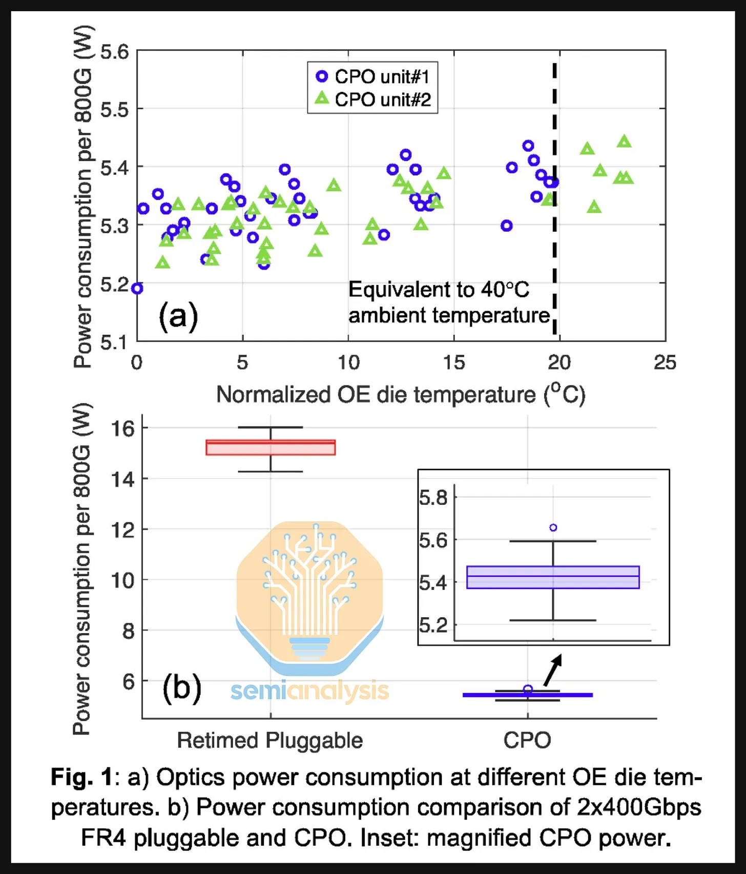
- The Meta–Broadcom Bailly research shown at ECOC 2025 reports ~15 W for an 800G 2xFR4 pluggable transceiver vs. 5.4 W for OE + laser source per 800G — a ~65% power saving on the same comparison.
(3) Effects analyzed at cluster level in scale-out
At the cluster level, the effect gets diluted.
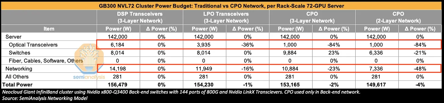
On a 3-layer GB300 NVL72 cluster, swapping DSP transceivers for CPO cuts transceiver power by 84% and networking power by 23%.
- But networking power is only ~9% of total cluster power.
- So a transceiver power -84% / networking power -23% reduction translates to roughly a 2% saving on total cluster power.
- A 2-layer CPO network can produce a larger networking-power reduction, but total cluster power saving still tops out at roughly 4%.
The same dilution shows up on the cost side.
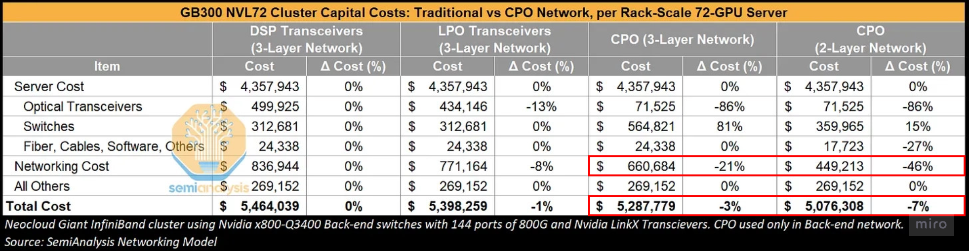
- On a 3-layer network, total networking cost can fall ~21% with CPO, but total cluster cost only drops ~3%.
- On a 2-layer CPO network, total networking cost can fall ~46%, but total cluster cost saving tops out at ~7%.
(4) Implications
- Scale-out CPO is a valid technology, but on its own it isn't enough to justify a fast hyperscaler adoption curve.
- A 3–7% total cluster cost saving and a 2–4% total cluster power saving aren't enough to override the burdens of serviceability, reliability, and vendor lock-in.
3. Why Scale-up is the More Strategic Case
| Scale-up | Scale-out | Scale-across |
|---|---|---|
| GPU-to-GPU within a local compute cluster | Rack-to-rack within a cluster (between rack switches) | Between geographically separated datacenters |
| 1–2 m, ultra-low latency, ultra-high bandwidth | 1 to tens of m (intra-rack / rack-to-rack), across the cluster fabric | Kilometer scale, between GW datacenter halls / sites |
| NVLink, NVLink Fusion, ESUN, UALink | Backend optical transceivers + spine / leaf | 800G, 1.6T optical transceivers (direct deployment) |
- Scale-out CPO is a cost / power problem.
- Scale-up CPO is a physics-and-architecture problem.
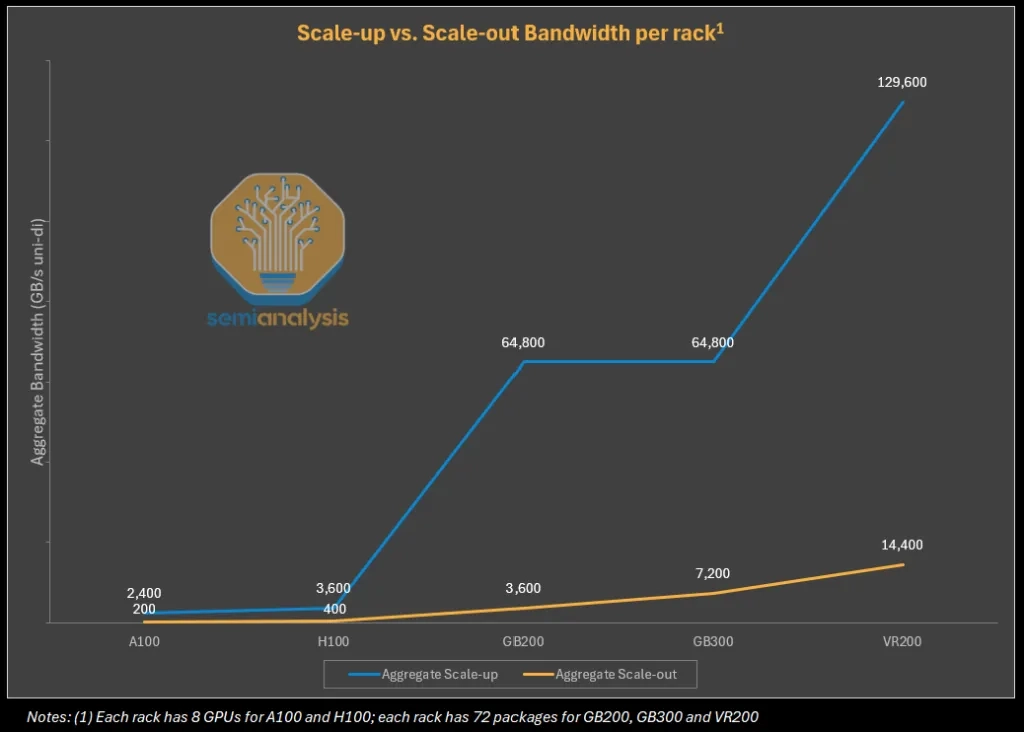
- The scale-up fabric demands far higher bandwidth and far lower latency than the back-end scale-out network.
- Scale-out: in the GB300 NVL72's back-end scale-out network with a CX-8 NIC, that's 100 GByte/s (800 Gbit/s) per GPU.
- Scale-up: Nvidia Blackwell NVLink delivers 900 GByte/s (7,200 Gbit/s) per GPU — roughly 9× scale-out.
(1) Implications of the NVLink 5.0 → 6.0 transition
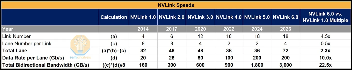
- NVLink 6.0's total bandwidth (TBW) doubles vs. 5.0 (1,800 GB / s → 3,600 GB / s).
- From NVLink 2.0 through 5.0, total bandwidth was lifted by doubling per-lane data rate. Starting with NVLink 6.0, per-lane data rate stays fixed and the total lane count is doubled instead.
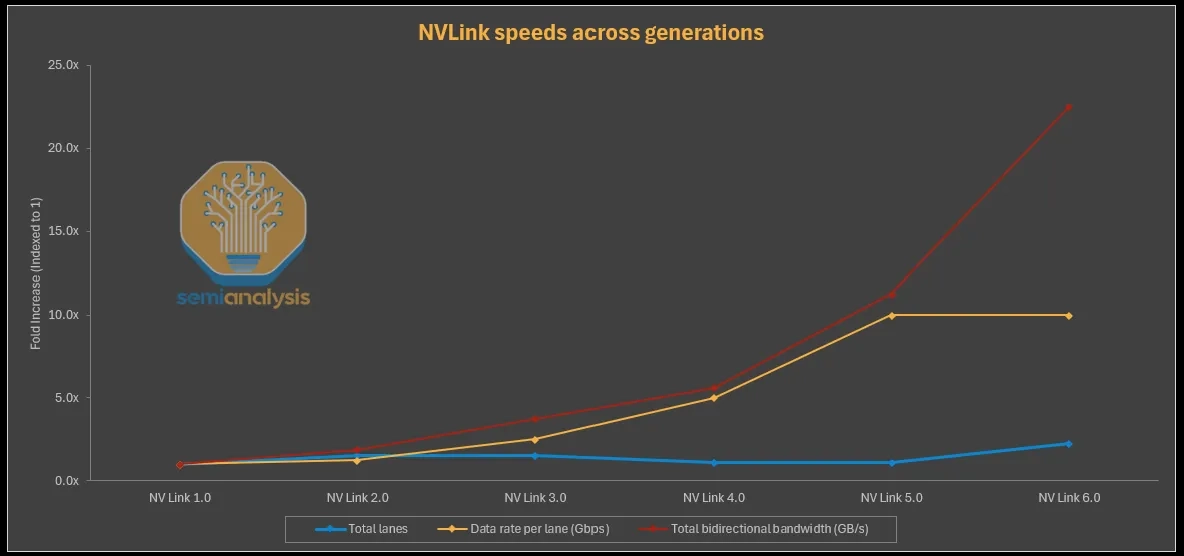
Reading the chart intuitively, doubling total bandwidth requires raising either per-lane speed or lane count.
- Through NVLink 5.0, aggregate bandwidth was scaled by raising in-link signal density and SerDes rate while keeping or growing the number of links per GPU each generation.
- That is, NVLink 6.0's defining shift is not lane-speed-only scaling — it is shoreline bandwidth-density scaling, where the package / rack spine has to handle 2× the link / port / escape density to double the lane count.
The longer the current engineering structure holds, the heavier the bandwidth-scaling burden on the next-generation NVLink.
- Doubling total bandwidth requires one of two levers: more lanes, or higher per-lane data rate.
- Both levers are running into physical limits.
- Per-lane data rate runs into SerDes power, copper loss, and signal integrity;
- lane count runs into package shoreline, bump pitch, and routing density.
- Even NVLink 6.0's lane increase is not a simple physical-lane doubling.
- The total lane count appears to grow from 36 to 72,
- but the structure is closer to keeping the same 36 physical copper lanes and using bi-directional SerDes to double effective lane count.
- That is, two signals are sent simultaneously on the same physical copper wiring, doubling effective lane count without adding shoreline.
- It's an engineering workaround for the lane-count constraint — and at the same time a sign that the existing electrical fabric is approaching its physical scaling limits.
NVLink is a critical strategic asset for NVIDIA.
- If total bandwidth stalls, Nvidia's scale-up moat narrows.
- With AMD and other hyperscalers building their own scale-up solutions, raising interconnect speed is the only survival option.
- The technology that opens the next stage of scale-up is exactly CPO adoption.
(2) How CPO defends NVLink's bandwidth moat
CPO defends NVLink's bandwidth moat by shrinking the electrical distance ahead of optical conversion.
The problem with the existing electrical fabric isn't simply "copper vs. light"; it's that high-speed electrical signals have to travel too far. CPO places the optical engine right next to the ASIC, dramatically shortens that electrical path, and changes the nature of the problem.
- Existing structure: long electrical channel with heavy equalization burden.
- The electrical signal traverses PCB traces, connectors, and the module — and along that long path, loss, crosstalk, reflection, and equalization burden compound.
- CPO structure: very short electrical path before optical conversion.
- Because optical conversion happens close to the ASIC, electrical distance shrinks from centimeter scale to millimeter scale.
- The result:
- The same bandwidth can be delivered at lower drive strength and lower power, opening room to design for higher per-lane speeds or wider I / O interfaces.
Implications
CPO looks like an enabling technology that relaxes NVLink's SerDes-power, signal-integrity, and shoreline constraints, extending the scale-up bandwidth moat.
4. The Bottleneck Moves to Packaging
(1) The CPO optical engine isn't a single chip — it's an electro-optical system pairing PIC and EIC
A PIC (Photonic Integrated Circuit) is the optical circuit that modulates, transmits, splits, combines, and detects light. An EIC (Electronic Integrated Circuit) is the circuit that drives, amplifies, equalizes, and controls electrical signals. Relative to the ASIC, the signal flows like this:
- Tx: switch ASIC → EIC → PIC → fiber.
- Rx: fiber → PIC → EIC → switch ASIC.
The crux of the optical engine in CPO is not just bonding a photonics chip next to the ASIC. The PIC (handling light) and EIC (handling electrical signals) have to operate in concert, and how short and low-parasitic the electrical interface between the two dies is determines performance.
The PIC–EIC parasitics problem
- The legacy issue: PIC–EIC parasitics.
- Every electrical connection between PIC and EIC carries unwanted
- capacitance (storing electrical charge — at high speeds, this creates needless charging / discharging burden, dragging on speed and power efficiency),
- inductance (resistance to changes in current — at high speeds, this can introduce latency, ringing, and noise),
- resistance (dissipates energy — causes signal attenuation, power loss, and heat). Together these are called parasitics.
- Every electrical connection between PIC and EIC carries unwanted
- The core packaging challenge: a minimum-parasitic PIC–EIC interconnect.
- The longer the connection between PIC and EIC, or the more bumps / TMVs / traces it has to pass through, the worse signal loss, power consumption, latency, and signal integrity get.
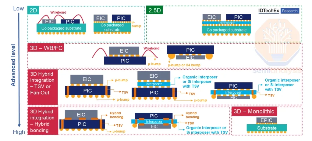
Packaging spectrum and CPO's trade-offs
- What good CPO packaging requires: a short, dense, clean electrical interface.
- The shorter and denser the PIC–EIC connection, the higher per-lane speeds, lower drive strength, and better signal integrity you can achieve.
- There are two main routes for connecting them.
- Monolithic integration: fab PIC and EIC on the same wafer.
- Heterogeneous integration: fab PIC and EIC separately, then combine in package.
- Heterogeneous integration is becoming the mainstream path:
- Monolithic integration makes the joining step easy and minimizes parasitics, latency, and power consumption.
- But silicon-photonics process can't really shrink below ~35 nm.
- Modern EICs require precise CMOS at 7 nm, 5 nm, 3 nm, etc. A 35 nm-bound EIC can't push CPO speed and performance to maximum.
- It ends up being more sensible to apply the CMOS process best suited to each — PIC and EIC — and to optimize each independently.
The packaging spectrum matters because the packaging structure dictates interconnect length, density, and bonding method, and the resulting parasitics directly govern bandwidth, power efficiency, latency, and signal integrity.
In general, going from 2D → 2.5D → 3D stacking → hybrid bonding shortens and densifies inter-chip connections, lowers parasitics, and improves electrical performance.
- 2D side-by-side (top left): simplest and easiest to implement, but the inter-chip interface path is long and parasitics are high — the worst on bandwidth, power, and signal integrity.
- 2.5D side-by-side on an interposer (top right): the interposer offers shorter and cleaner connections, raising I / O density and bandwidth and improving signal integrity.
- 3D stacking / TSV / fan-out: stacking dies vertically dramatically shortens trace lengths, lowering parasitics and enabling higher bandwidth density and lower latency.
- Hybrid bonding: direct bonding without µ-bumps (the orange dots between EIC and PIC) achieves the finest pitch, minimizing resistance, capacitance, and power loss — best in class for electrical performance.
(2) TSMC COUPE (Compact Universal Photonic Engine)
This is where TSMC COUPE's strategic importance comes in.
- COUPE bundles PIC fabrication, EIC fabrication, SoIC hybrid bonding, optical coupling, and fiber attachment into a single stack.
- TSMC's edge is in providing leading-edge CMOS, SoIC, and an advanced-packaging ecosystem in one place.
The crux of COUPE is stacking PIC and EIC directly via SoIC, removing the parasitics bottleneck of FOWLP / TMV structures.
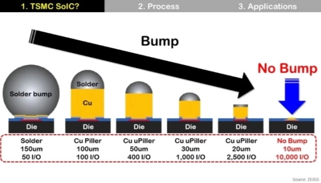
In COUPE, PIC and EIC are stacked using TSMC's SoIC and bumpless bonding. The traditional µ-bump approach connects two dies through solder bumps; SoIC removes those solder bumps and brings the two dies into direct copper-to-copper contact.
| Existing structure | COUPE structure |
|---|---|
| µ-bump / FOWLP / TMV-based connections | SoIC-based bumpless direct bonding |
| Intermediate structures like bumps, mold, and vias sit between PIC and EIC, lengthening the electrical path and increasing parasitic capacitance, inductance, and resistance. | PIC and EIC are connected vertically and directly, minimizing trace length and removing unnecessary solder-bump and TMV paths. |
- Key principle: shorter traces = lower parasitics = better performance.
- Shorter electrical paths improve bandwidth, power efficiency, and signal integrity.
- What SoIC means: the shortest heterogeneous connection achievable in a non-monolithic structure.
- Short of fully integrating PIC and EIC into one chip, SoIC is about as close as you can get to the shortest, densest way to connect heterogeneous dies.
Broadcom TH5 Bailly's FOWLP approach and its limits
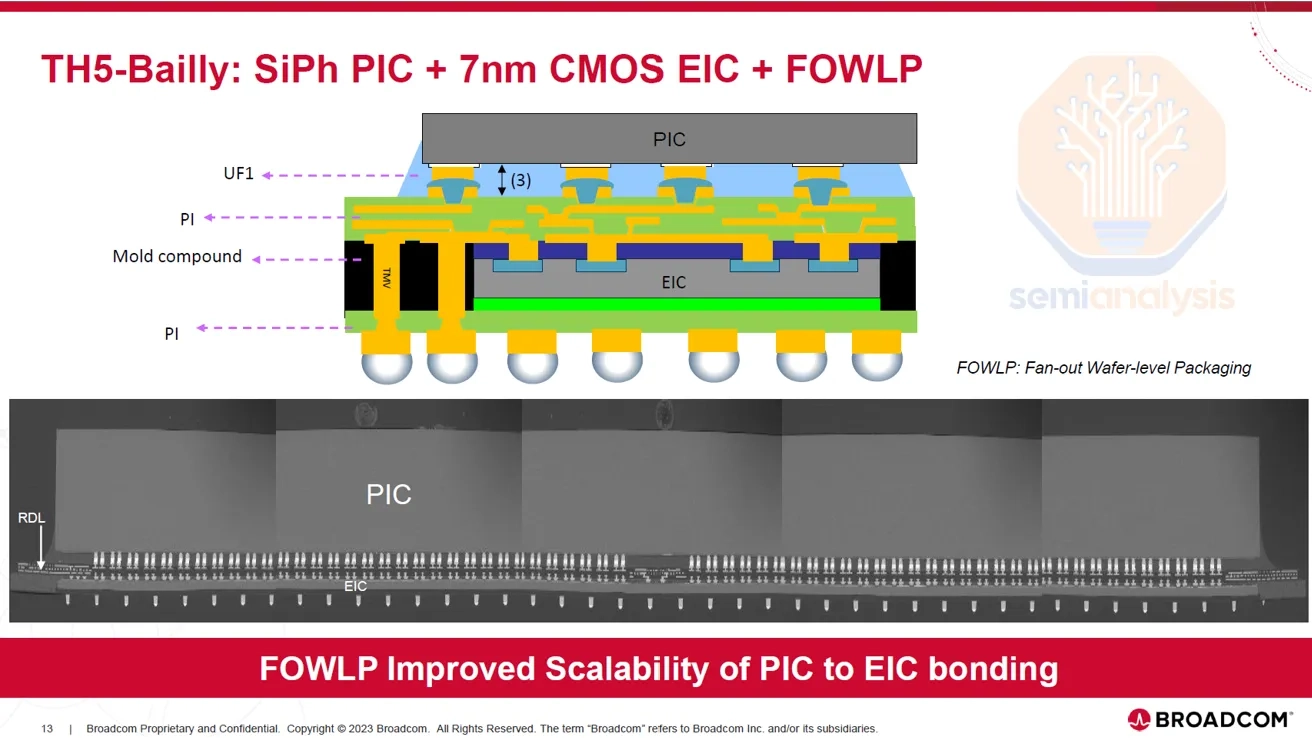
Broadcom's Bailly CPO (TH5 generation) uses FOWLP packaging.
- Structurally, the SiPh PIC sits on top, the 7 nm CMOS EIC on the bottom, and the two are connected via TMVs (Through-Mold Vias).
- The problem: TMVs are vertical interconnects through mold compound.
- Compared to bumps, TMVs make for a longer electrical path and induce parasitic capacitance because of the dielectric properties of the surrounding mold.
- These parasitics degrade eye margin, insertion loss, and signal integrity at high speeds, and ultimately bottleneck lane speed at the 100G / lane level.
- Above 100G, the degradation that comes from passing through mold compound grows in scale, and so do power and equalization burdens.
COUPE vs. Broadcom TH5 Bailly
| Item | COUPE SolC | Broadcom TH5 Bailly CPO |
|---|---|---|
| Packaging | 3D integration based on SolC / hybrid bonding | FOWLP (Fan-Out Wafer-Level Packaging) |
| Die structure | EIC-PIC vertical integration | PIC on top, EIC on bottom |
| Connection method | Direct bonding / fine-pitch interconnect | TMV (Through-Mold Vias) |
| Bottleneck | Removes the TMV | TMV parasitic capacitance |
| Performance ceiling | Favorable for > 100G / lane scaling | Signal degrades past 100G / lane |
(3) The two coupling methods inside COUPE
1) Edge Coupling
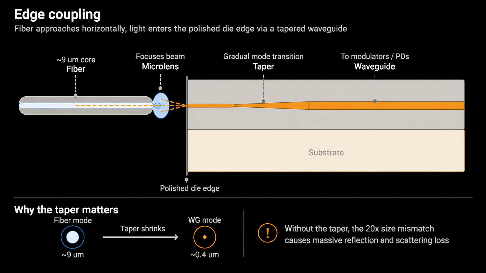
- Edge coupling has the fiber approach the side — the edge — of the chip, injecting light into the waveguide.
- A microlens at the fiber tip narrows the beam, and a tapered waveguide at the chip edge smoothly converts the fiber mode into the on-chip waveguide mode. (The "wide light bundle" arriving via fiber is gently compressed into the "narrow light channel" inside the chip.)
| Item | Detail | What it means for CPO |
|---|---|---|
| Advantages | Coupling loss (the optical power lost when light passes from fiber into the chip waveguide due to alignment error, mode mismatch, reflections) is low | Light transfers efficiently from fiber to chip waveguide, helping the optical power budget |
| Strong broadband behavior (performance stays stable across a wide wavelength range) | Operates stably across a wide wavelength range, favoring WDM (Wavelength Division Multiplexing) designs | |
| Low polarization sensitivity | Less sensitive to changes in input-light polarization, raising link stability | |
| Strong optical alignment | Smoothly compresses the "wide light bundle" arriving via fiber into the "narrow light channel" inside the chip | |
| Disadvantages | Fibers must be arranged in a 1D row along the chip edge | High-density 2D fiber-array attach is hard, capping fiber density (one coupling can attach only one fiber) |
| Requires die-edge processing (precisely machining the chip side for optical coupling) | Increases process complexity | |
| Advanced packaging processes don't always mate cleanly with fiber | Hard to dovetail with die stacking, wafer thinning, TSV, and interposer integration | |
| Mechanical reliability burden is high | With fiber attached directly to the chip edge, assembly, handling, and shock / vibration become risks | |
| Hard to mass-produce | Precision alignment, bonding, and inspection make yield and cost management harder |
2) Grating Coupling
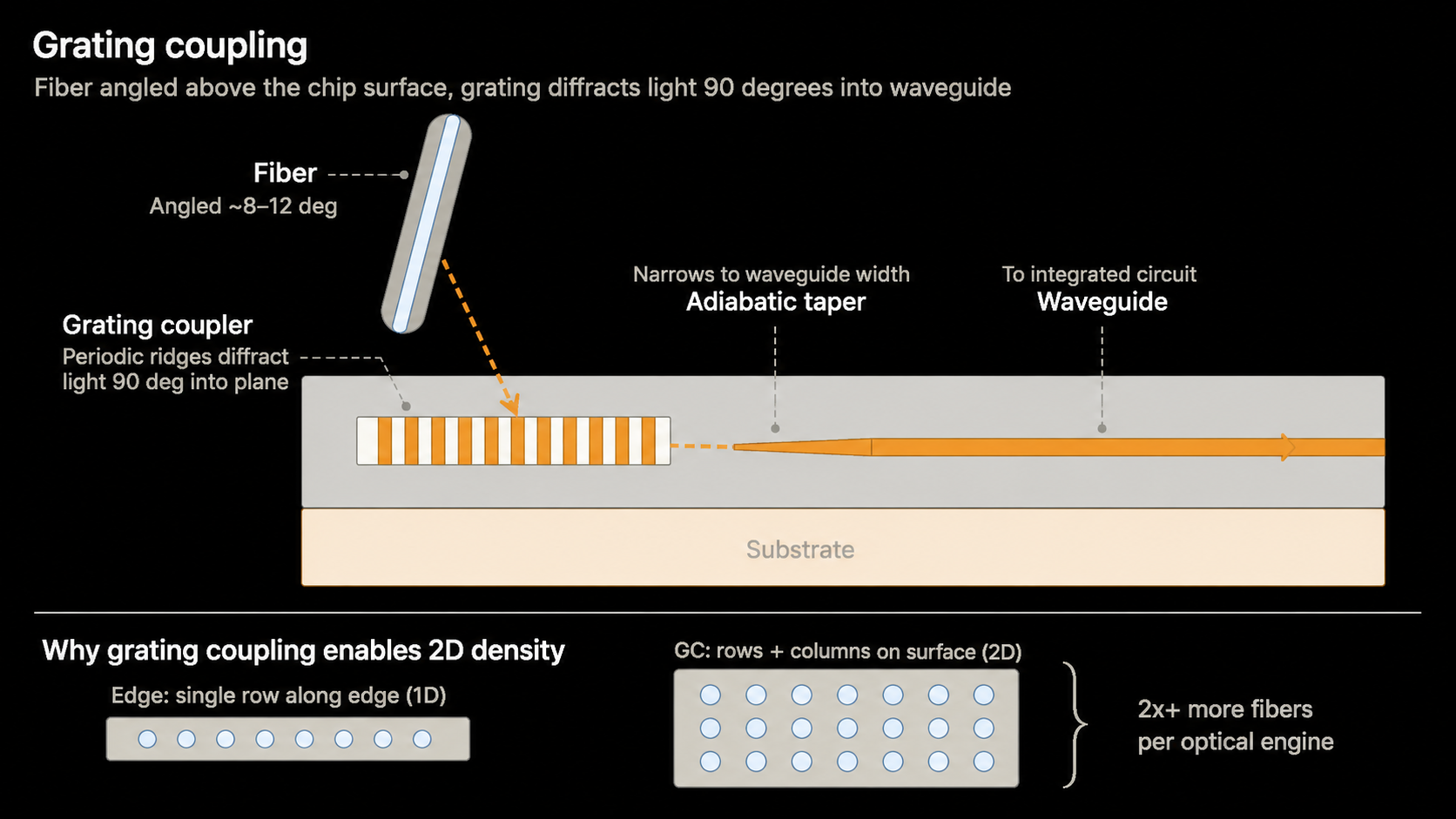
- A coupling method whose strengths lie more in density and manufacturability than in raw optical performance.
- The fiber approaches from above the chip; a grating structure on the chip surface diffracts vertically incident light into the horizontal direction of the waveguide.
- The grating effectively acts like an optical antenna, bending light entering from above into the chip plane.
- An adiabatic taper then progressively shapes the beam to match the waveguide width.
| Item | Detail | What it means for CPO |
|---|---|---|
| Advantages | Fibers can approach from above the chip surface | Fiber position isn't tied to the die edge, raising layout flexibility |
| 2D fiber arrays are possible | Easier to achieve higher fiber density than edge coupling (beyond 1D, 2D density is achievable) | |
| The coupler doesn't need to live at the die edge | Reduces die-edge processing burden and increases chip-placement flexibility | |
| Wafer-level testing is comparatively easy | Optical test can run at the wafer stage before dicing, helping yield management | |
| Better fit with advanced packaging | Easier to combine with interposer, 2.5D / 3D packaging, and optical-engine integration roadmaps | |
| Disadvantages | Higher coupling loss than edge coupling | Tightens the optical power budget and raises laser-power requirements |
| Narrower wavelength bandwidth | Harder to operate stably across wide wavelength ranges, putting pressure on WDM design | |
| Polarization sensitivity | Coupling efficiency varies with input-light polarization | |
| Grating design is wavelength-specific | Tends to be optimized for specific wavelengths, limiting design margin | |
| Vertical-to-horizontal conversion loss | Diffraction loss occurs while light entering from above gets bent into the chip plane |
3) Why do Nvidia and TSMC prefer grating coupling?
The logic for Nvidia and TSMC favoring grating coupling isn't about an absolute optical-performance advantage — it's about implementing CPO as a high-density, mass-manufacturable package.
- The choice of coupling method in CPO is no longer just "lowest optical loss"; it becomes "how much I / O density can be implemented in a manufacturable way."
- Edge coupling is favorable on optical performance, but because fiber has to be arranged in a 1D row along the chip edge, a CPO structure where one optical engine demands tens of fiber connections quickly hits a density wall.
- Existing issue: density limit of 1D edge-only coupling.
- Edge coupling needs side-of-chip access, restricting fiber placement to along the edge.
- As the fiber count of CPO optical engines grows, this becomes a bottleneck on package layout and fiber density.
- Grating coupling's strength: 2D fiber grid.
- Because fibers approach from above the chip, they can be arranged on the chip surface as a 2D grid. That fits the high-density optical I / O CPO requires.
- Fit with the CoWoS / interposer roadmap.
- When the optical engine sits on a CoWoS interposer, you can't always guarantee that the chip edge stays exposed or accessible.
- Edge coupling needs an exposed edge; grating coupling injects light from above, giving package layout more flexibility.
- Core trade-off: optical efficiency vs. density / manufacturability.
- Edge coupling delivers lower coupling loss and a cleaner optical signal.
- Grating coupling can have higher optical loss but makes a denser, more manufacturable CPO package.
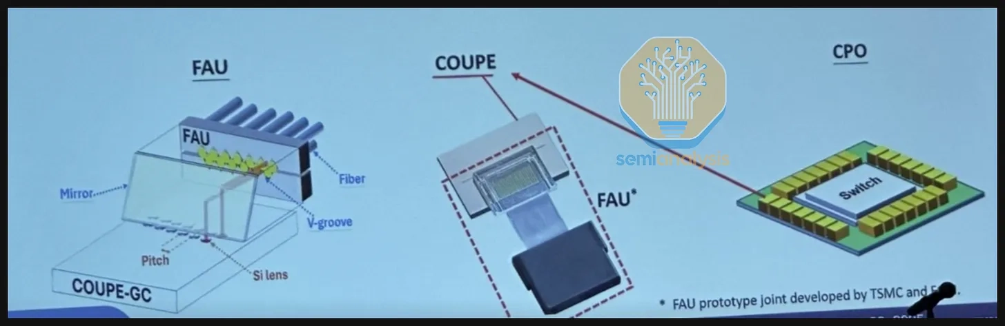
(4) FAU (Fiber Attach Unit)
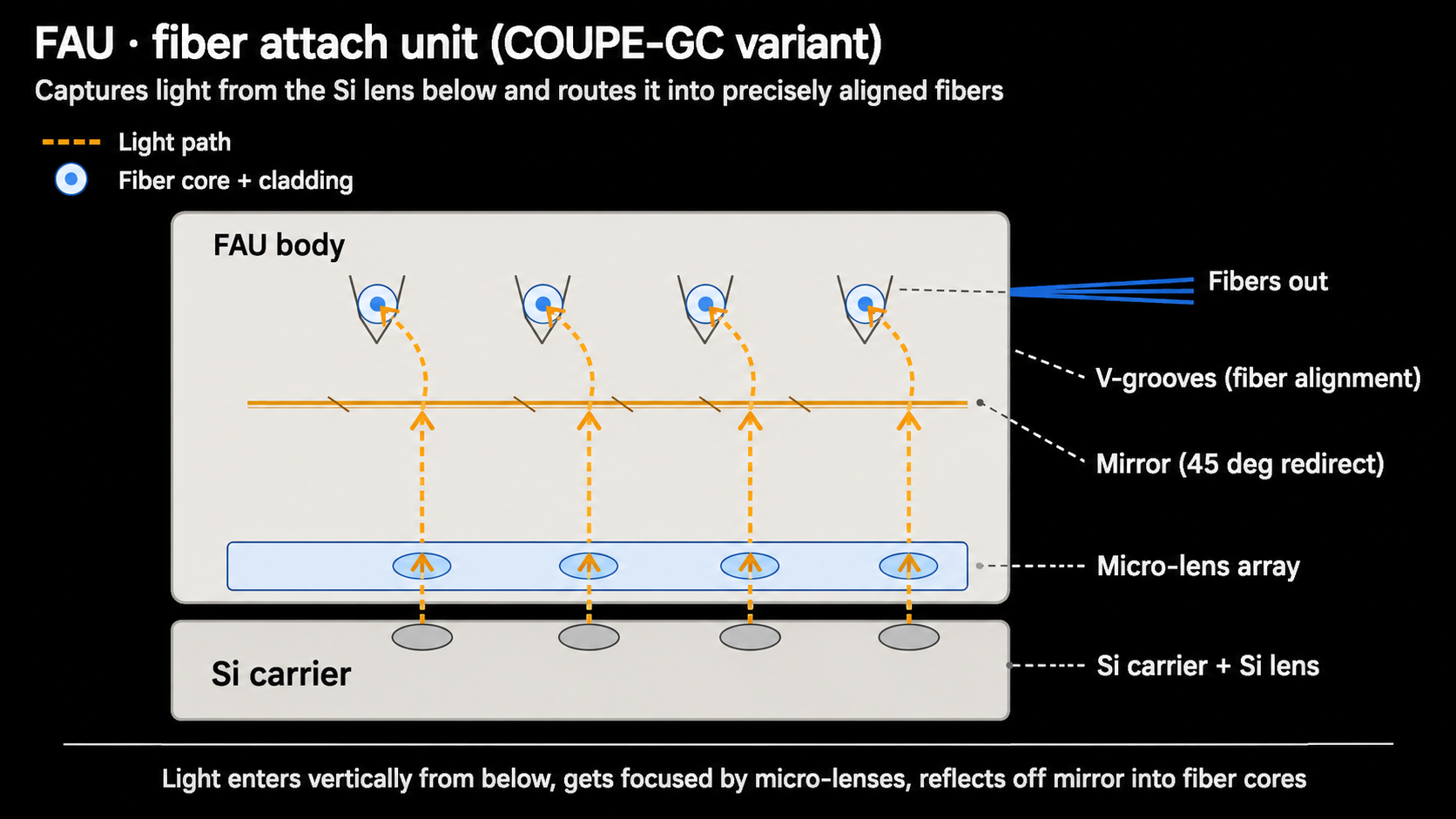
- The FAU is the physical bridge between the optical engine and external fiber.
- Even if the PIC can generate or detect light, the optical link doesn't form unless that light actually lands precisely in the fiber core.
- The FAU's role: optical alignment + beam shaping.
- The FAU rigidly holds the fiber array in place and uses micro-lenses or mirrors to focus or redirect the beam.
Light path inside the grating-coupling structure
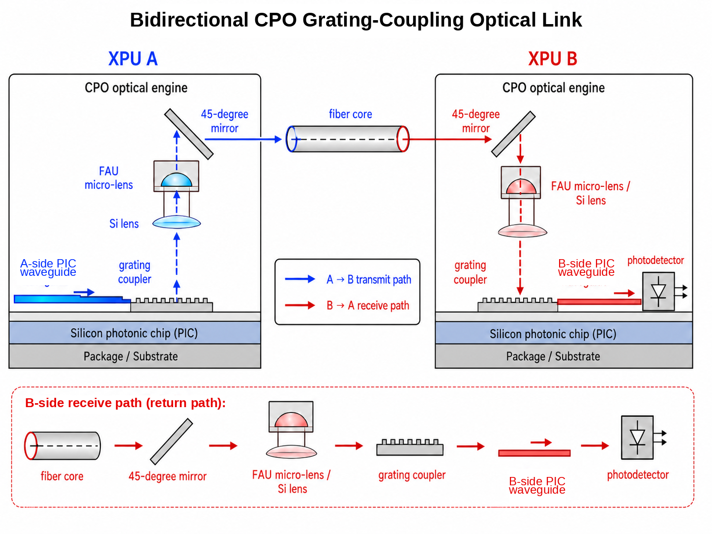
Suppose XPU A and XPU B are interconnected via CPO.
- Light path (A → B): A's PIC waveguide → grating coupler → Si lens → FAU micro-lens → 45° mirror → fiber core.
- Light path (B → A): fiber core → 45° mirror → FAU micro-lens / Si lens → grating coupler → B's PIC waveguide → photodetector.
- Fiber-fixing scheme: V-groove alignment.
- Fibers are precisely fixed in V-grooves. The V-groove mechanically stabilizes fiber position, helping the beam land on the center of the fiber core.
- Core difficulty: alignment tolerance.
- Single-mode fiber cores are about 9 µm wide, so even a few µm of misalignment can push light off the core and dramatically increase insertion loss.
- Manufacturing implication.
- So the FAU is not a simple optics component; it's a precision-manufacturing problem combining micron-level alignment, lens / mirror assembly, fiber attach, and bonding reliability.