On CPO Pt.1 | The Phased Transition from Pluggables to CPO
Before getting into the main parts, this briefing-style opener covers the conclusion, the core summary, and the five-step spectrum of optics moving closer to the chip (Pluggables → LPO → OBO → NPO → CPO).
Conclusion
- CPO (Co-Packaged Optics) is hard to frame simply as "a technology that reduces networking power and cost."
- A more accurate investment frame:
- Scale-out CPO has clear per-unit power savings vs. optical transceivers, but cluster-level TCO improvement is bounded.
- Scale-up CPO carries more strategic weight in the regime where copper / SerDes scaling is approaching physical limits.
- In other words, CPO adoption is more likely to bifurcate by use case than to roll out uniformly.
- In scale-out networking, TCO, serviceability, reliability, and interoperability can throttle the pace of adoption.
- In scale-up AI interconnect, bandwidth density and escape-bandwidth bottlenecks make CPO's strategic necessity much greater.
Core Summary
Before going specific, GPU networking splits along three axes.
| Scale-up | Scale-out | Scale-across |
|---|---|---|
| GPU-to-GPU within a local compute cluster | Rack-to-rack within a cluster (between rack switches) | Between geographically separated datacenters |
| 1–2 m, ultra-low latency, ultra-high bandwidth | 1 to tens of m (intra-rack / rack-to-rack), across the cluster fabric | Kilometer scale, between GW datacenter halls / sites |
| NVLink, NVLink Fusion, ESUN, UALink | Backend optical transceivers + spine / leaf | 800G, 1.6T optical transceivers (direct deployment) |
- Scale-up: GPU-to-GPU within a local cluster (1–2 m, ultra-low latency / ultra-high bandwidth, NVLink, etc.).
- Scale-out: rack-to-rack / intra-cluster (tens of meters, backend transceivers + spine / leaf).
- Scale-across: between geographically separated datacenters (kilometer scale, direct deployment of 800G / 1.6T transceivers).
- This article focuses on scale-up and scale-out.
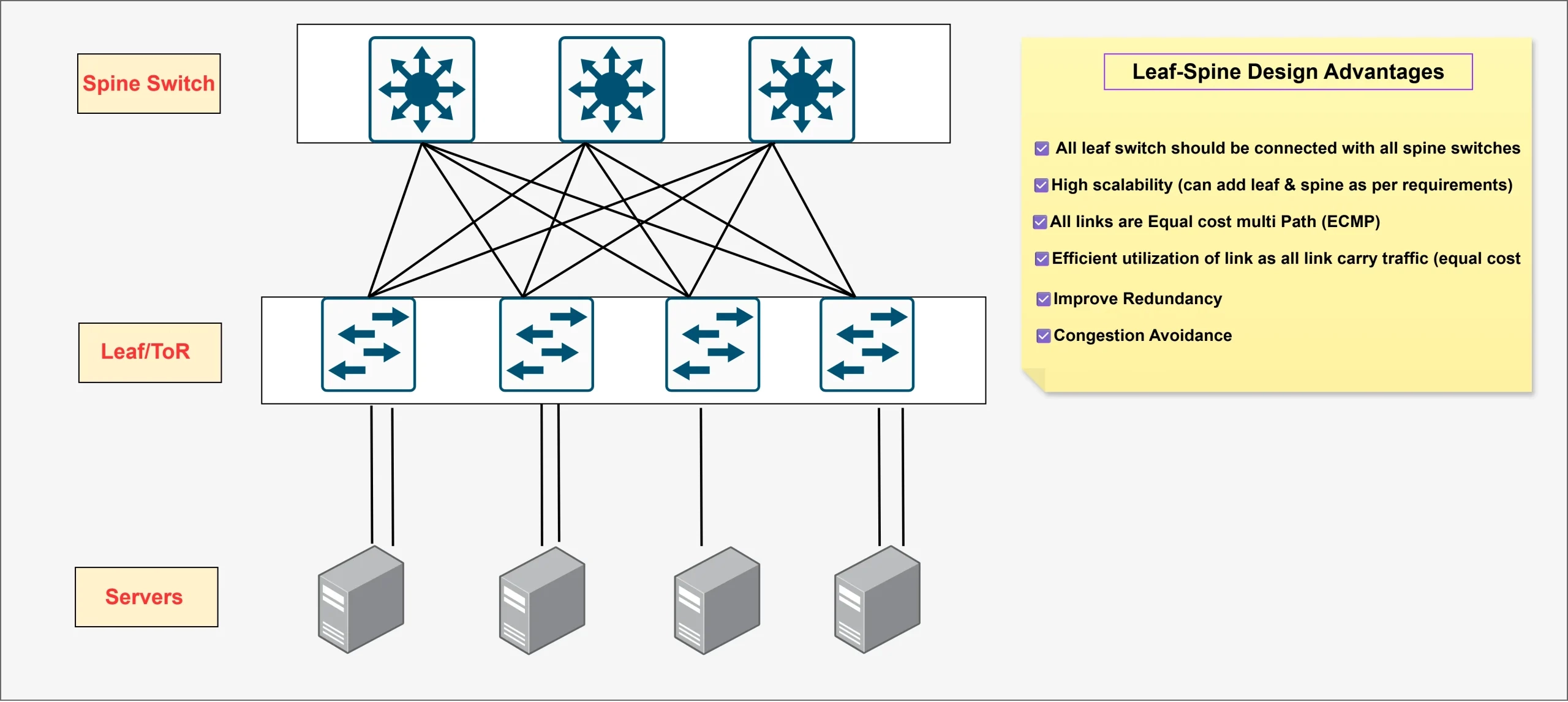
Reference: scale-out networking structure.
(1) The limits of legacy copper & optical-transceiver networking, and what CPO implies
Copper-based scale-up links offer high bandwidth but short reach.
- NVLink delivers very high per-GPU bandwidth, but the copper distance constraint (~2.2 m) means a pure-copper network design caps the scale-up domain at roughly one or two racks.
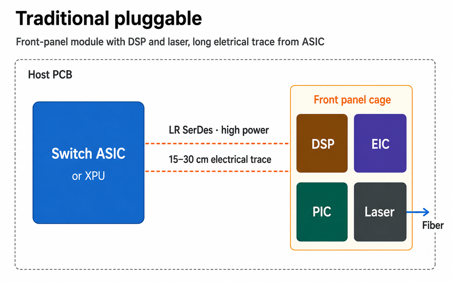
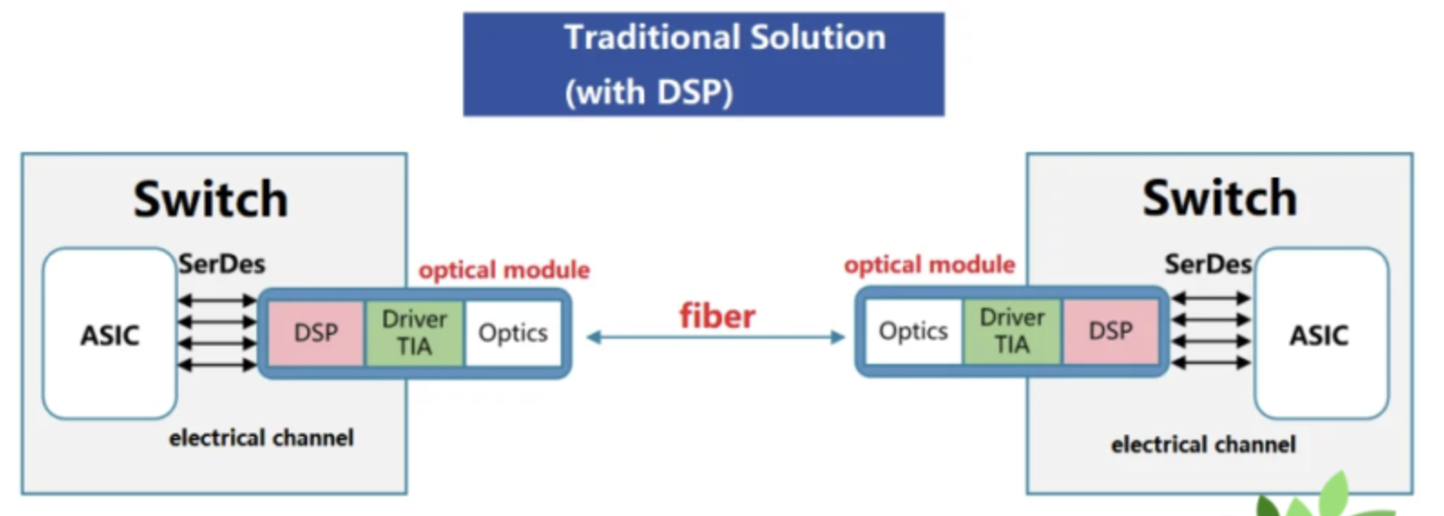
Traditional pluggable transceivers solve the reach problem, but the electrical trace the signal has to traverse before optical conversion is long.
- The transceiver module sits in the front-panel cage, 15–30 cm away from the XPU / switch ASIC.
- Data moves as ultra-high-speed electrical signals along the PCB and connectors into the module's DSP, where the DSP / EIC / PIC convert it to an optical signal and push it onto fiber.
- That long electrical path drives connector / PCB losses and inflates the burden on power, latency, and signal integrity.
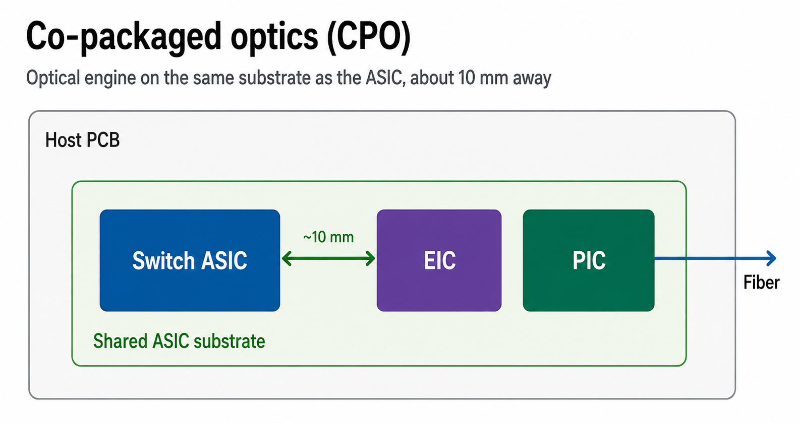
CPO compresses the long electrical path between ASIC and optical engine into the package itself. By placing the optical engine right next to the ASIC — on the same package or substrate — it dramatically shortens the distance the electrical signal has to travel.
- The optical engine sits next to the ASIC.
- Unlike traditional pluggables, the signal does not travel out to a module at the edge of the board; it converts to optical right by the ASIC.
- The electrical path shrinks.
- Long PCB traces and connector segments shrink, reducing signal loss, parasitics, and equalization burden.
- DSP can be removed or downsized.
- Once the electrical path is short, heavy retiming / equalization is less necessary, and in some architectures DSP-less or DSP-light designs become viable.
- That said, not all CPO removes DSP entirely.
- Lower-power short-reach SerDes can replace LR SerDes.
- Pluggables have to cross the board and connectors, so they need stronger long-reach SerDes;
- CPO's short ASIC–to–optical-engine distance can make do with lower-power SerDes.
(2) CPO's scale-out vs. scale-up economics
CPO's scale-out economics may not look as compelling as the component-level power savings suggest.
- At the optical-module or switch-device level, CPO shrinks the electrical path and delivers significant power savings.
- But once you zoom out to cluster level, networking is only one slice of total power and cost — compute, memory, cooling, and system integration carry larger weights.
- So CPO's device-level efficiency gains do not translate 1:1 into final TCO improvement.
The stronger strategic case is in scale-up interconnect. Scale-up hinges on extremely high-bandwidth, low-latency GPU / XPU connectivity, so the physical limits of electrical interconnect bind more directly. NVLink and other high-bandwidth electrical fabrics are getting squeezed on two scaling levers simultaneously.
- Per-lane speed: pushing per-lane rates higher worsens SerDes loss, power, and signal-integrity problems.
- Shoreline / lane count: even if you want more lanes, package edge, bump pitch, and routing density constrain how many you can fit.
⇒ CPO's role: place the optical engine close to the ASIC and reduce the electrical distance from centimeter scale to millimeter scale.
So in scale-out, CPO is closer to a power-saving story; in scale-up, it is closer to an architecture story that reopens the bandwidth-scaling runway.
(3) The vendor race is not just a photonics-IP contest
CPO winners aren't decided purely by whether you can design a good SiPh PIC. The crux is the packaging / manufacturing capability to bond the optical engine reliably next to the ASIC and ship it in volume-manufacturable form.
- Packaging: how short and low-parasitic you can keep the EIC–PIC–ASIC interconnect.
- Fiber attach: process stability for aligning and fixing many fibers at the package boundary.
- External laser integration: how you supply the laser source and manage coupling loss / reliability.
- Thermal control: the ability to isolate ASIC heat from the optics so it doesn't compromise performance and reliability.
- Manufacturing yield: how high you can drive the composite yield of optics + EIC + packaging + assembly.
That's why the center of gravity of the CPO race shifts to the combination of photonics design + advanced packaging + high-volume manufacturing. The strategic importance of the TSMC COUPE / SoIC stack lies less in being a "packaging technology" per se than in being the integration platform that can turn CPO and scale-up optical fabric into shippable products.
1. Pluggable → LPO → OBO → NPO → CPO: The Phased Migration of Optics Toward the Chip
CPO does not arrive overnight; it sits at the end of a spectrum along which optics keeps moving closer to the chip. Reading that spectrum makes it much clearer "why now" CPO is happening and "by what path" it gets here.
Background: The layered hierarchy of chips
Die (chip) → Substrate (protects and connects the die) → Package → PCB (connects packages) → Motherboard / system.
- The PCB is the device-wide "floor."
- The substrate is a specialized "mini-floor" right beneath an individual chip (or chip group), sitting on top of the PCB.
These terms matter because in CPO discussions, phrases like "same package," "on substrate," and "next to the ASIC on PCB" each refer to a different layer.
(1) Where copper stops
- Copper handles the bandwidth bands where it can, and optics takes over wherever copper becomes inefficient.
- At 200G per lane (1.6T transceiver), copper becomes hard to manage on losses, power, and signal integrity.
- For DAC alone, 200G per lane makes spanning even the 2.2 m of a single server rack difficult — which is why Nvidia is targeting an aggressive transition to optics from 200G per lane (3.2T transceiver).
The four tiers of copper interconnect
Copper remains efficient at short reach, but the faster per-lane speeds get, the harder physical limits bite — power growth, distance-dependent attenuation, and degrading signal integrity.
| Type | Structure | Characteristics |
|---|---|---|
| PCB trace | The most basic electrical wiring connecting chips inside a board / module | Connection distances are typically a few cm. At short distances, high-frequency PCB materials and careful design preserve signal integrity. |
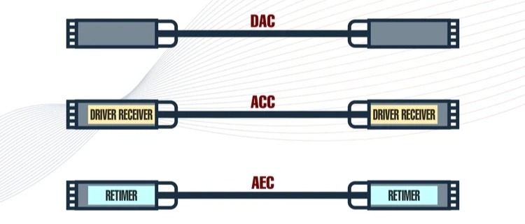
| DAC (Direct Attach Copper) | Passive copper cable made of just copper wire and insulator, with no signal-processing chips at either end | Suited for very short runs under ~1 m. Low cost, near-zero power, and the most economical short-distance link. |
| ACC (Active Copper Cable) | A linear analog equalizer at each end partially compensates for loss | Better signal compensation than DAC, supports ~2–3 m. Avoids the complex digital chips of AEC, so power efficiency is good. |
| AEC (Active Electrical Cable) | Electrical cable with digital signal-processing chips (DSP or retimer) at each end | Aggressively corrects insertion loss / crosstalk / return loss. Supports higher rates and 3–7 m, making it a very widely used short-reach interconnect for 400G / 800G server racks. |
The deeper driver: compute is overtaking I / O
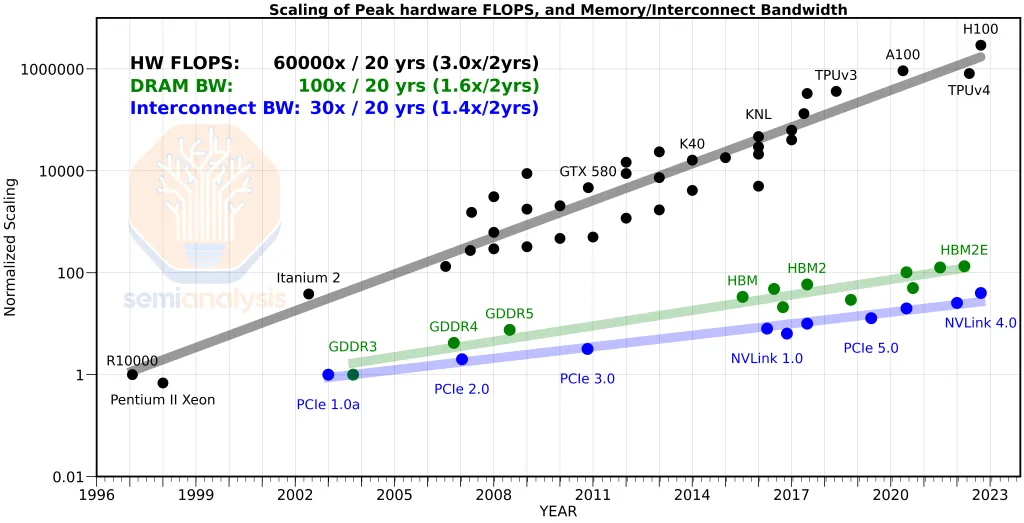
The most fundamental driver in the CPO discussion isn't simple efficiency improvement; it's the structural gap between compute, which scales exponentially, and I / O, which doesn't.
- Black: hardware FLOPS — exponential growth.
- Green: DRAM bandwidth — incremental growth.
- Blue: interconnect bandwidth — nearly flat.
I / O struggles to scale for three reasons that compound:
- Package shoreline limits: substrate perimeter and bump density are physically capped.
- Difficulty raising per-lane speed: pushing per-lane bit rates demands more power and more complex SerDes, and signal integrity degrades non-linearly.
- Plateau in flip-chip BGA bump count: HPC packages' off-package I / O density is already near the ceiling.
These compound into a ceiling on escape bandwidth — the maximum data per second that can leave a package.
(2) The inefficiency DSP creates
The most direct meaning of "pluggables are inefficient" is DSP.
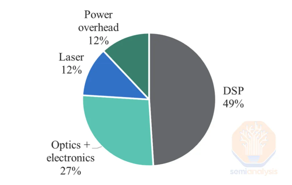
The dominant cost / power burden in a traditional pluggable transceiver is the DSP.
- In a 30 W pluggable transceiver, the DSP alone consumes about 20 W — roughly 50% of total module power.
- On a BoM basis, about 20–30% of the transceiver cost lives in the DSP.
- The result: transceivers can account for ~10% of cluster TCO, and roughly half of that is the DSP.
Why DSP is needed
- The signal has to traverse 15–30 cm of lossy PCB from the XPU / switch ASIC to the front-panel module.
- Once the electrical signal has crossed that distance, it needs retiming, error correction, and clock / data recovery before it can be converted to optical.
- In other words, DSP is a recovery circuit for a structural problem: a long electrical path.
How big does that burden get at cluster scale?
- A single GB300 NVL72 rack-scale server houses 72 Grace-Blackwell GPUs.
- Those 72 GPUs form a single rack-scale compute domain via NVLink / NVSwitch-based scale-up networking.
- Each NVL72 rack connects to other racks via InfiniBand / Ethernet scale-out networking, and many racks together make up a cluster.
Power basis
So cluster size is fundamentally "rack count × 72 GPUs."
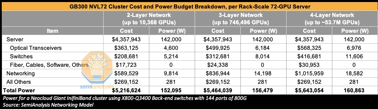
- For a 10,368-GPU GB300 cluster + 2-layer InfiniBand network:
- GB300 NVL72 is a 72-GPU unit, and each GPU connects to the network via one 800G NIC, so 10,368 800G DR4 transceivers are used for the GPU / SuperNIC → leaf-switch link.
- On the switch side, one 1.6T DR8 handles two 800G links, so 5,184 GPU-facing leaf-side + 10,368 leaf-spine fabric-side = 15,552 total 1.6T DR8 transceivers are used.
- Note that these numbers follow SemiAnalysis's counting convention: 800G DR4 covers GPU / SuperNIC-side endpoints, and 1.6T DR8 includes the physical OSFP modules on the leaf-switch and spine-switch sides.
- DSP power assumptions: 6–7 W per 800G DSP, 12–14 W per 1.6T DSP, giving:
- 800G DSP: 10,368 × 6–7 W ≈ 62–73 kW.
- 1.6T DSP: 15,552 × 12–14 W ≈ 187–218 kW.
- Total DSP: ~249–290 kW; midpoint ~270 kW.
- For a 10,368-GPU cluster on 72-GPU rack-scale servers:
- Server count = 10,368 / 72 = 144.
- DSP power per server = 270 kW / 144 ≈ 1.87 kW per 72-GPU server.
- So per GPU server rack, DSP burns about 1.87 kW ≈ 1,872 W.
- As the table above shows, total networking power for a 10,368-GPU GB300 cluster + 2-layer InfiniBand network is 9,814 W per rack.
- 1,872 / 9,814 = 0.19; about 19% of networking power is consumed by DSP.
TCO basis
- When sourcing transceivers from premium brand-name suppliers, transceivers can account for nearly 10% of total cluster TCO.
- A typical transceiver has DSP at ~50% of power consumption and ~20–30% of BoM,
- So some treat DSP as one of the largest bottlenecks on cost and power efficiency.
What CPO solves
- CPO shrinks the electrical path to mm-scale, nearly eliminates the retiming burden, and as a result lets you remove or radically simplify the DSP.
- DSP removal is the largest single source of CPO's ~50–80% power-saving claim.
- That's why some analysts have called DSP "public enemy number one for cost and power efficiency."
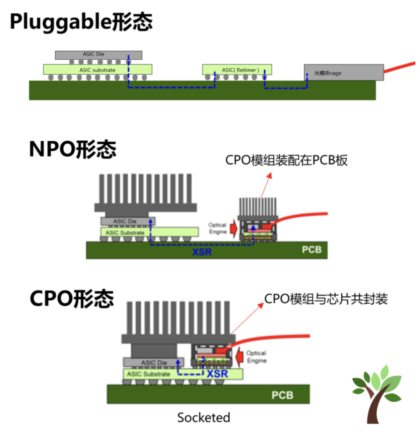
(3) Side-by-side: Pluggable → LPO → OBO → NPO → CPO
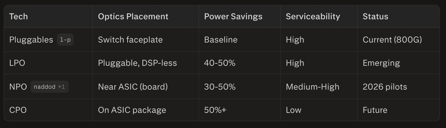
| Stage | Optics Location | DSP Required? | Serviceability | Power (approx.) |
|---|---|---|---|---|
| Traditional Pluggables | Front-panel cage (15–30 cm) | Required (long PCB path) | Front-panel hot-swap | 30 W per module |
| LPO (Linear Pluggable) | Same front-panel cage | Removed (host absorbs the burden) | Front-panel hot-swap | 15–18 W per module |
| OBO (On-Board Optics) | Mid-board, on the PCB (a few cm) | Still required | Soldered → field swap difficult | ~20 W per module |
| NPO (Near-Packaged) | Separate package next to ASIC (on PCB) | Can be simplified | Module-level replaceable | ~15 W per 800G |
| CPO (Co-Packaged) | Same substrate as ASIC (~10 mm) | Removed or substantially shrunk | Package-level replacement | ~5 W per 800G |
How to think about LPO's place
- OBO / NPO / CPO are progressive shortenings along the physical-proximity axis.
- LPO does not move along that axis — it's an orthogonal variation that strips the DSP within the same pluggable form factor.
- So LPO is a "variant of pluggables," not a stage in line with OBO / NPO / CPO. Shown as five stages side by side, LPO belongs to a different axis at the same layer.
LPO (Linear Pluggable Transceivers) structure
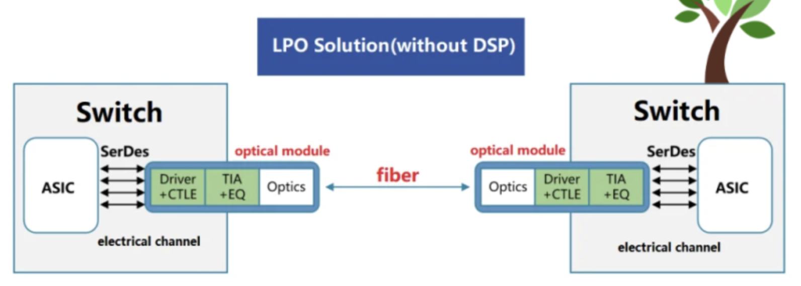
- Keeps the front-panel cage module form of traditional pluggables, but removes the in-module DSP and shifts the signal-processing burden to the host.
- The module itself becomes a "linear" path with only a driver + CTLE + EQ + TIA.
- Pros: direct power savings from DSP removal, lower latency, and preserved front-panel hot-swap serviceability.
- Cons: the compensation work that once lived in the module moves to the host, so the host chip needs to be more capable, and deployment requires tighter management. This is why LPO is treated as a partial power-saving option rather than a wholesale replacement for pluggables.
OBO (On-Board Optics) structure
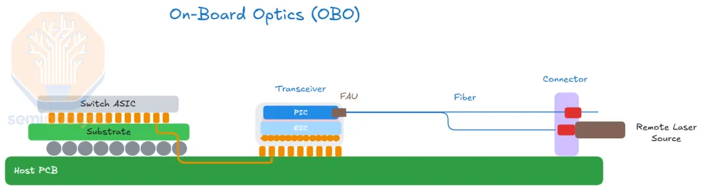
- The optical module is soldered to mid-board near the ASIC instead of sitting in the front-panel cage.
- The electrical signal still travels a few cm along the PCB, so DSP is still required.
- Light leaves the OBO module via an internal fiber jumper that routes to the front-panel connector.
- A middle stage between pluggables and NPO — it pulls optics close to the chip but does not put it on the same substrate as the ASIC.
NPO (Near-Packaged Optics) structure
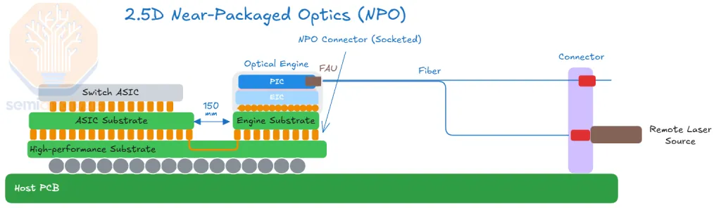
- ASIC and optical engine sit side by side on the same PCB but in separate packages.
- The signal still traverses a few cm of PCB, but far less than front-panel pluggables or OBO.
- The optical engine is replaceable / swappable via a socket / interposer separate from the ASIC.
- Power efficiency runs roughly 50% of pluggables (~30 W → ~15 W).
- Manufacturability / serviceability: harder than front-panel pluggables, but much easier than full CPO.
NPO as a bridge to CPO
- CPO designs struggle to keep the laser source stable in a hot environment, so they pair naturally with ELS (External Laser Source), which keeps the laser outside.
- For optical-transceiver companies, going via NPO rather than directly to CPO makes more sense in terms of manufacturability, supply chain, and qualification.
- Nvidia is also targeting CPO directly as the primary path, but maintains a roadmap that routes through NPO to CPO if production proves difficult.
(4) The other path: CPC (Co-Packaged Copper)
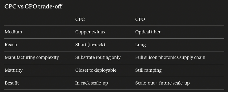
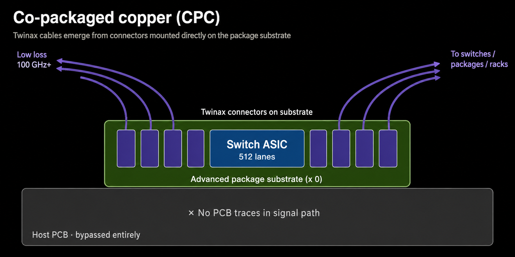
CPC is another answer to the same "long lossy electrical path" problem.
- The defining feature is that the connector is soldered onto the package substrate itself rather than the PCB.
- The cable exits straight from the connector next to the ASIC, bypassing the lossy PCB-trace section entirely.
- The cable is twinax (twin-axial) — a well-insulated copper pair with dramatically lower insertion loss than PCB trace.
Existing "flyover" cables also bypassed parts of the lossy PCB section, but they still started from a socket on the PCB. CPC moves the socket itself onto the package, so the path never touches the PCB to begin with.
CPC vs. CPO
- CPC and CPO are two different answers to the same problem — "the long lossy electrical path."
- CPC: keep using copper, but on a shorter path and a better medium (twinax).
- CPO: cut the electrical path to mm-scale and convert to optical altogether.
- Nvidia maintains a "use copper where you can, optical when you must" stance, so CPC is more likely on short / intra-rack runs and CPO on longer ones.
- CPC is the signal that "copper isn't dead." A CPC + CPO hybrid — not a CPO-only narrative — is the realistic picture of future production systems, which is why Broadcom and Nvidia both run the two paths in parallel.
(5) Implications
- CPO adoption is more likely to be a phased migration than a "pluggables → CPO" jump.
- Each intermediate stage (LPO, OBO, NPO) can settle in as a generation's production product in its own right.
- The biggest forces accelerating this phased path are DSP power + the compute-vs-I / O scaling gap + the per-lane SerDes ceiling.
The two phases of scale-up CPO: Phase 1 (rack-to-rack) → Phase 2 (intra-rack)
Scale-up CPO further breaks into two phases:
| Phase | Timing | Mechanism |
|---|---|---|
| Phase 1 — Rack-to-Rack Scale-up CPO | 2H27 (Nvidia Rubin Ultra) | Copper cables can't go past 3 m, so pod-level domains like NVL72×8 = NVL576 or NVL144×8 = NVL1152 get connected over fiber. The simple copper → optical swap delivers ~3–4× performance gains per unit of traffic. |
| Phase 2 — Intra-Rack Scale-up CPO | 2H28+ (around Nvidia Feynman) | Past 400G per lane, copper hits its limits even inside the rack — cost, power, and distance constraints fire simultaneously. Optics fills the intra-rack, rack-to-rack, spine, and DCI domains all at once. Crossing into the rack is roughly a 10× jump in optical-lane demand. |
- This framing reframes CPO adoption from a "one-shot event" to a multi-year migration whose penetration depth differs by generation.
- Why scale-up has higher adoption potential than scale-out is taken up in Part 2.