On CPO Pt 4 | Today's Major CPO Products
A look at Nvidia (Quantum-X / Spectrum-X) and Broadcom (Humboldt / Bailly / Davisson) production CPO product lineups, Nvidia's generation-by-generation adoption timeline, and a comparison of the two vendors' entry paths.
On CPO
- Part 1, The Phased Transition from Pluggables to CPO
- Part 2, The Economic and Architectural Case for CPO
- Part 3, Inside the Optical Engine
- Part 4, Today's Major CPO Products
- Part 5, OCS, Testing, and the Optical Value Chain
8. Today's Major CPO Products
- The vendors actually driving the production CPO roadmap are essentially two — Nvidia and Broadcom.
- Both ultimately converge on the TSMC COUPE platform, but their paths to get there and their architectural choices differ sharply.
(1) Nvidia (NASDAQ: NVDA)
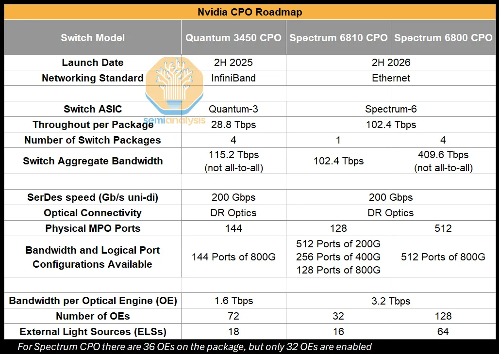
| Switch | Standard | Launch | Aggregate BW | OE BW |
|---|---|---|---|---|
| Quantum X800-Q3450 | InfiniBand | 2H 2025 | 115.2 Tbps | 1.6 Tbps |
| Spectrum 6810 | Ethernet | 2H 2026 | 102.4 Tbps | 3.2 Tbps |
| Spectrum 6800 | Ethernet | 2H 2026 | 409.6 Tbps | 3.2 Tbps |
Nvidia's CPO roadmap splits in two phases. Quantum-X is a first-gen product aimed at supply-chain validation; Spectrum-X is closer to a more aggressive architectural bet.
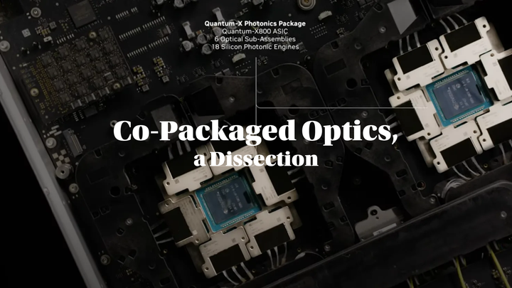
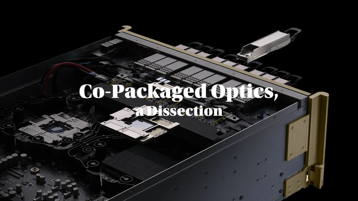
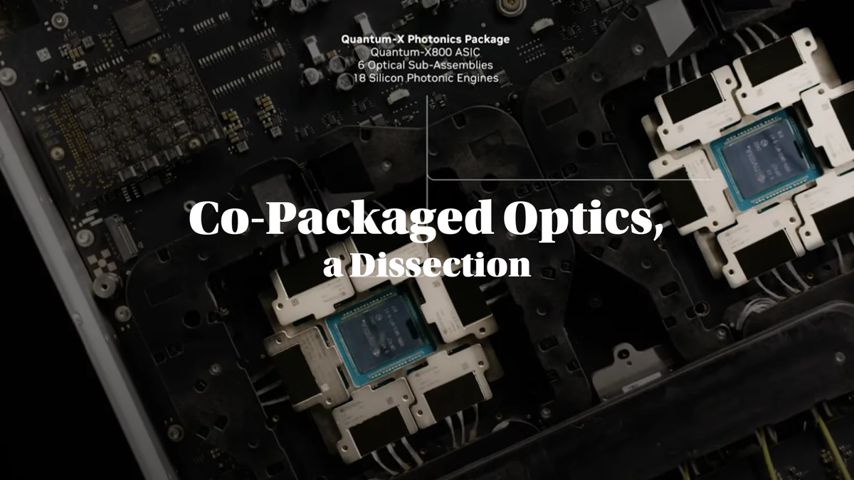
1) Quantum X800-Q3450
Quantum X800-Q3450 — Nvidia's first-gen production CPO switch.
- Standard: InfiniBand
- Launch: 2H 2025
- Aggregate BW: 115.2 Tbps
- OE BW: 1.6 Tbps (Gen 1)
- Architecture: 4 monolithic ASICs, multi-plane
Multi-plane architecture
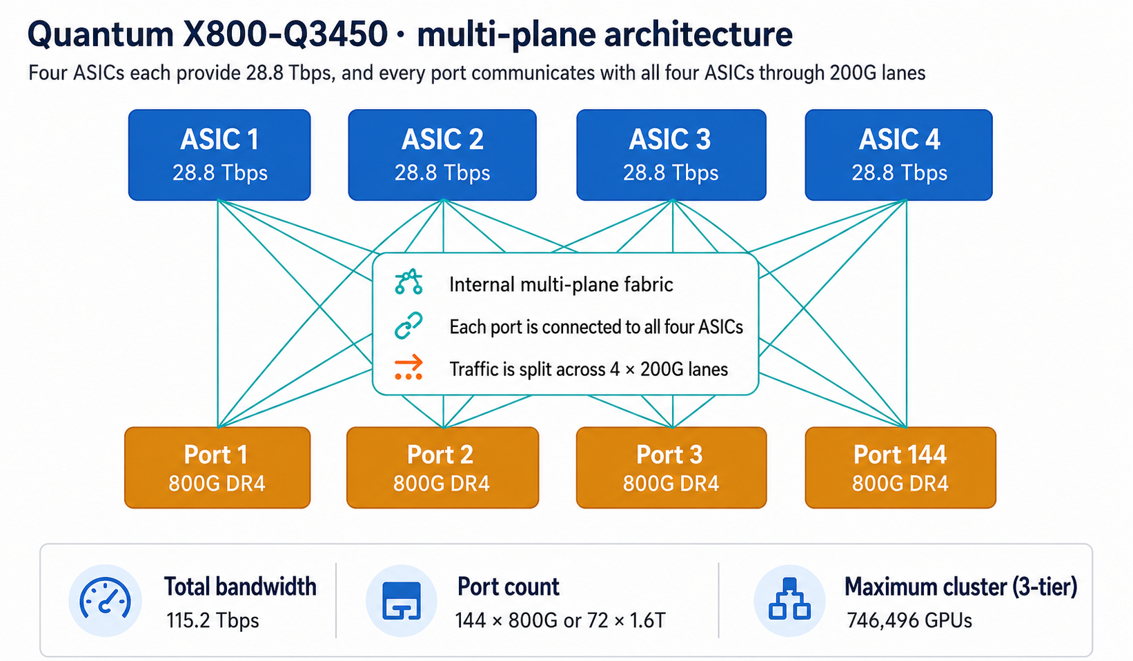
The crux of Quantum-X is multi-plane architecture.
- Each 800G physical port splits into 4 × 200G lanes, with each lane connecting to a different ASIC.
- Data is sprayed across all four ASICs and recombined at the destination port.
- The result reaches the same maximum cluster size as four discrete 28.8T switches (746,496 GPUs at 3 tiers), but the shuffle happens inside the box, dramatically reducing external fiber complexity.
Inside the package
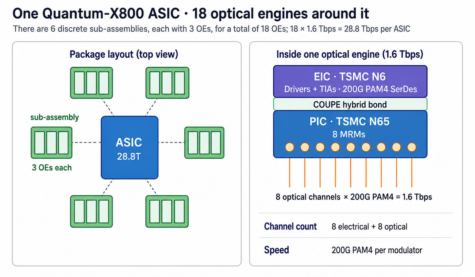
- Each of the four ASICs is surrounded by six detachable optical sub-assemblies, with each sub-assembly containing three optical engines.
- Per ASIC: 18 OE × 1.6 Tbps = 28.8 Tbps.
- Across the package: 4 ASIC × 18 OE = 72 OE, 4 × 28.8T = 115.2 Tbps aggregate.
- The detachable sub-assembly matters — technically it leans closer to NPO and lowers the serviceability burden vs. full CPO.
The 200G MRM breakthrough
- Quantum-X's most important engineering claim is that each MRM operates at 200G PAM4 (8 modulators × 200G = 1.6 Tbps per engine).
- That matches the fastest MZMs and overturns the industry assumption that "MRM is stuck at NRZ."
- It is an engineering achievement by Nvidia + TSMC, and it simultaneously justifies the MRM-centric strategy.
Process-node split
- The PIC is fabricated on N65 (a mature node). Optical components gain little from scaling and tend to perform more stably at larger geometries.
- The EIC is fabricated on N6 (an advanced node). For driver, TIA, and control logic, the density and power-efficiency benefits of advanced nodes are clear-cut.
- The two dies are connected at sub-micron interconnect granularity via TSMC COUPE's hybrid bonding.
Cooling
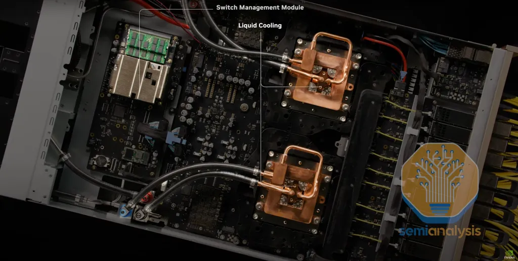
- Two copper cold plates sit on top of the ASIC in a closed-loop liquid-cooling configuration.
- It isn't only for ASIC thermals; it doubles as a mechanism to keep the temperature-sensitive MRM inside its narrow operating window.
Quantum-X implications
- Quantum-X is a supply-chain pipe-cleaner.
- Detachable sub-assemblies, smaller monolithic ASICs, and a relatively conservative 1.6T OE all make it a fault-tolerant first-gen product.
- If something fails, swap the sub-assembly. Nvidia gathers real-world reliability data without committing to a full-CPO architecture.
2) Spectrum-X Photonics
Spectrum-X Photonics — Nvidia's second-gen CPO switch (Spectrum 6810 / 6800).
- Standard: Ethernet
- Launch: 2H 2026
- Aggregate BW: 102.4 Tbps (6810) / 409.6 Tbps (6800)
- OE BW: 3.2 Tbps (Gen 2)
- Architecture: Multi-chip module (MCM)
Spectrum-X has a fundamentally different architecture from Quantum-X. Where Quantum-X is a multi-plane configuration of four monolithic ASICs, Spectrum-X is built around a much larger reticle-class multi-chip module (MCM).
- The 6810 is a single-package product using one MCM.
- The 6800 stitches together four 6810 MCMs (Spectrum-6 + 8 SerDes chiplets + OE set) inside a single chassis with built-in inter-package fiber shuffle, delivering 4× aggregate bandwidth.
Why MCM matters
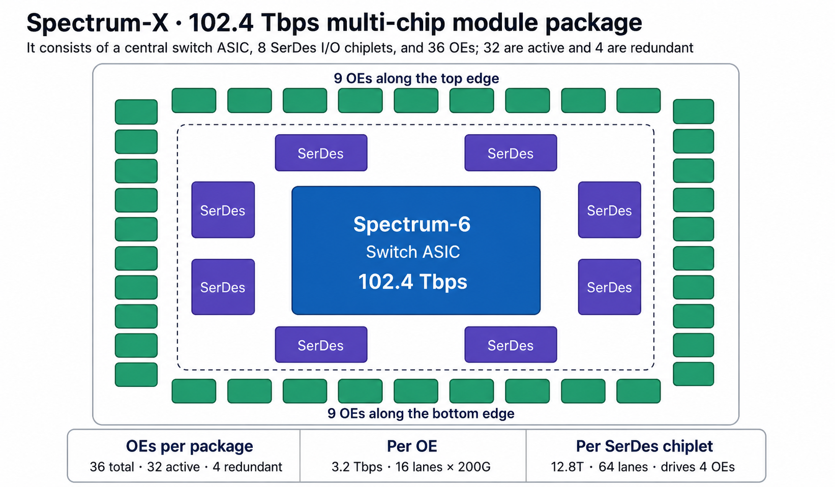
- The central Spectrum-6 switch ASIC is a 102.4 Tbps reticle-class die.
- Around it sit eight SerDes I / O chiplets (two on each side), each handling 64 × 200G lanes for 12.8T.
- This separation lets the design allocate far more shoreline to I / O than monolithic — the core reason for the 4× per-package bandwidth vs. Quantum-X.
3.2 Tbps optical engine (Gen 2)
- Each OE: 16 optical lanes × 200G.
- The package carries 36 OEs, but only 32 are active; the remaining 4 are redundancy.
- Unlike Quantum-X, the OEs are soldered to the substrate, so in-place replacement isn't possible. If an OE fails in the field, a spare OE has to take over.
- Each I / O chiplet feeds 4 OEs (12.8T per chiplet → 4 × 3.2T, a clean fan-out).
6810 vs. 6800
| Spec | Spectrum 6810 | Spectrum 6800 |
|---|---|---|
| Aggregate BW | 102.4 Tbps | 409.6 Tbps |
| MCM count | 1 | 4 |
| Physical ports | 128 × 800G | 512 × 800G |
| OE attachment | Soldered (true CPO) | Soldered (true CPO) |
| External lasers | 16 ELS | 64 ELS |
Spectrum-X implications
- Spectrum-X is an architectural bet.
- Soldered OEs (no field swap), 3.2T engines, MCM packaging accompanied by 8 SerDes chiplets — a far more aggressive design.
- The design is premised on the supply chain Quantum-X is currently building.
- The four redundant OEs are essentially an architectural acknowledgement that "in the field, some fraction will fail, but in-place fixes are hard."
- 200G MRM is the foundational technology for both products and locks Nvidia onto the TSMC COUPE platform.
3) Quantum-X vs. Spectrum-X side by side
| Feature | Quantum X800-Q3450 | Spectrum 6810 | Spectrum 6800 |
|---|---|---|---|
| Standard | InfiniBand | Ethernet | Ethernet |
| Launch | 2H 2025 | 2H 2026 | 2H 2026 |
| Architecture | 4 monolithic ASICs (multi-plane) | 1 MCM | 4 MCMs in chassis (with fiber shuffle) |
| Per-ASIC / package BW | 28.8 Tbps per ASIC | 102.4 Tbps | 102.4 Tbps × 4 |
| Aggregate BW | 115.2 Tbps | 102.4 Tbps | 409.6 Tbps |
| OE bandwidth | 1.6 Tbps (Gen 1) | 3.2 Tbps (Gen 2) | 3.2 Tbps (Gen 2) |
| OE count | 18 per ASIC × 4 = 72 | 36 (32 active) | 36 (32 active) × 4 |
| OE attachment | Detachable (NPO-like) | Soldered (true CPO) | Soldered (true CPO) |
| Physical ports | 144 × 800G | 128 × 800G | 512 × 800G |
| External lasers | 18 ELS | 16 ELS | 64 ELS |
4) What the roadmap implies
- Quantum-X is the supply-chain pipe-cleaner.
- Detachable sub-assemblies, smaller monolithic ASICs, and a relatively conservative 1.6T OE make it fault-tolerant as a first-gen product.
- Failures get fixed by swapping the sub-assembly. Nvidia accumulates real-world reliability data without committing to a full-CPO architecture.
- Spectrum-X is the architectural bet.
- Soldered OEs (no field swap), 3.2T engines, MCM packaging with 8 SerDes chiplets — a much more aggressive design.
- The design depends on the supply chain Quantum-X is now building. The four redundant OEs are essentially an architectural acknowledgement that "in the field, some fraction will fail, but in-place fixes are hard."
- 200G MRM is the foundational technology for both products.
- Without that breakthrough, neither product hits its bandwidth target.
- At the same time, Nvidia is the first to ship 200G PAM4 MRM in production CPO — locking it onto the TSMC COUPE platform.
(2) Broadcom (NASDAQ: AVGO)
Broadcom is the longest-running production CPO vendor, having shipped three generations over four years.
| Generation | Switch ASIC | Announced | Aggregate BW | OE BW | # OEs | Key shift |
|---|---|---|---|---|---|---|
| Humboldt (TH4) | Tomahawk 4 | 2021 | 25.6 Tbps (half-electrical) | 3.2 Tbps | 4 | Proof of concept |
| Bailly (TH5) | Tomahawk 5 | OFC 2023 (2024 production) | 51.2 Tbps (all-optical) | 6.4 Tbps | 8 | Full CPO + CMOS EIC + FOWLP |
| Davisson (TH6) | Tomahawk 6 | October 2025 | 102.4 Tbps | 6.4 Tbps | 16 | TSMC N3, 200G / lane |
It's worth noting that all three generations are scale-out Ethernet switches. Broadcom has not yet entered InfiniBand or scale-up CPO production.
1) Generation 1: Humboldt (TH4) — Proof of Concept
Humboldt (TH4) — Broadcom's first-gen production CPO switch.
- Switch ASIC: Tomahawk 4
- Announced: 2021
- Aggregate BW: 25.6 Tbps (12.8T pluggables + 12.8T via 4 × 3.2T OE)
- OE BW: 3.2 Tbps × 4
Hybrid design
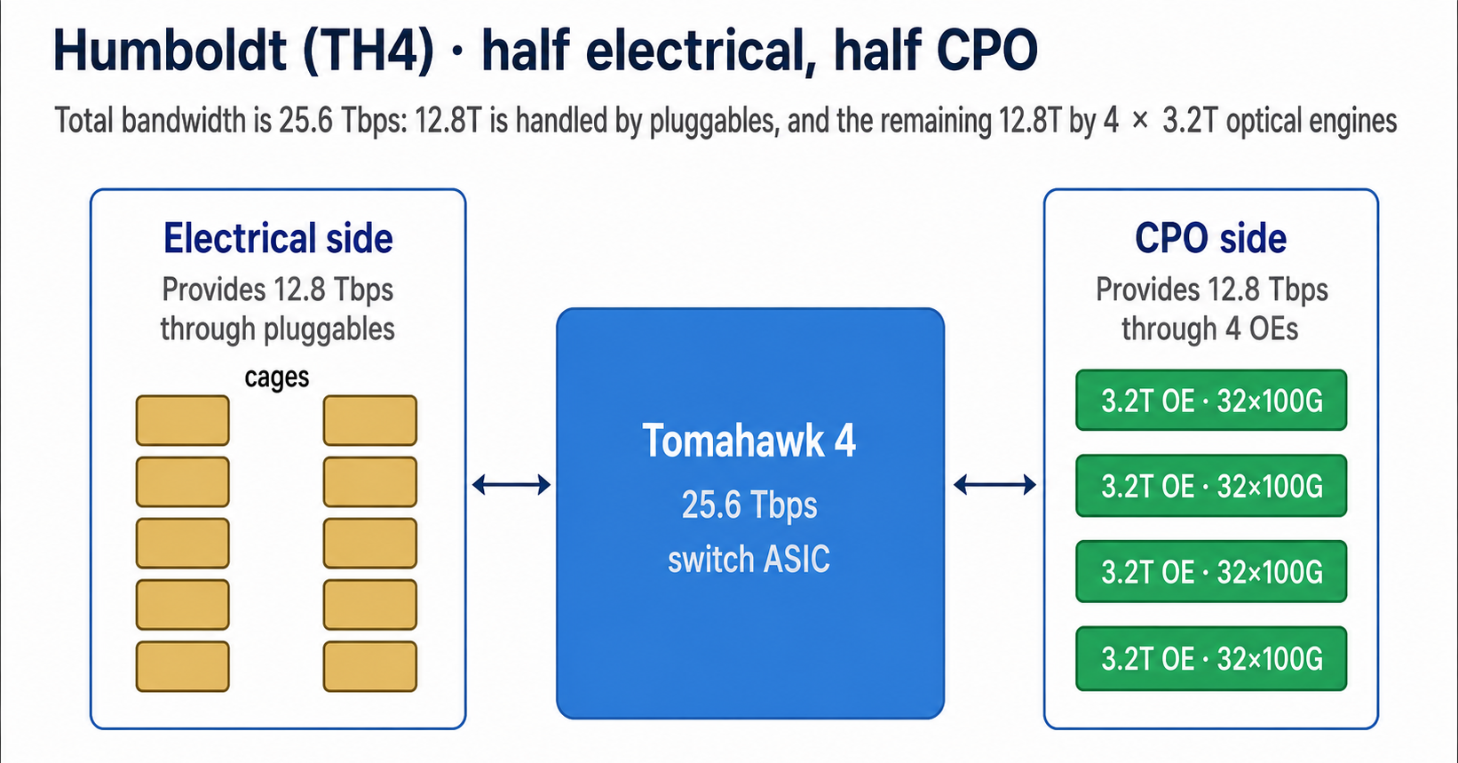
First-gen Humboldt was a hybrid design, splitting bandwidth in half between traditional electrical I / O and CPO.
- Why hybrid? A ToR switch needs both short copper links to servers (electrical) and long uplinks to spine switches (optical) at the same time. Splitting the switch this way let Broadcom validate CPO without committing the whole system to it.
Key technical choices
- PIC + SiGe EIC stacked via TSV process.
- SiGe carries a power penalty of about 3 pJ / bit vs. CMOS — one of the biggest reasons the next generation (Bailly) moved the EIC to CMOS.
- Roughly 250 optical components per OE — far fewer than the ~1,000 of subsequent generations.
Humboldt implications
- Humboldt proved CPO works in a real Ethernet switch.
- It also exposed the SiGe EIC's power penalty, giving Broadcom a clear motivation to move to 7 nm CMOS in the next generation.
- It's closer to a proof of concept than the formal start of production CPO.
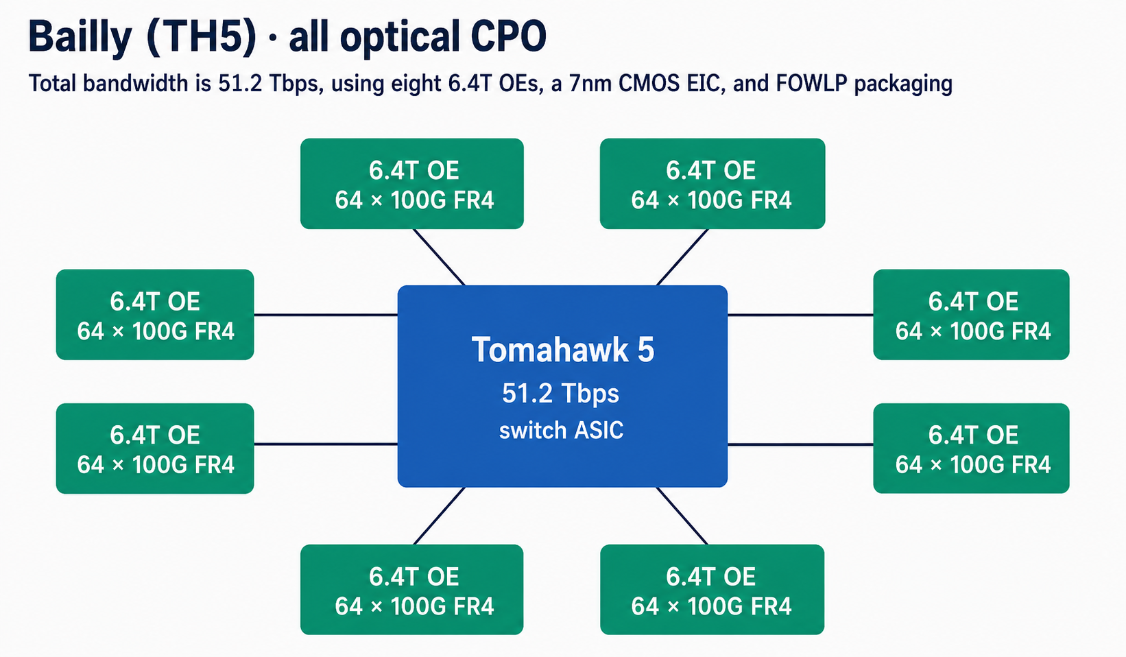
2) Generation 2: Bailly (TH5) — Full Optical CPO
Bailly (TH5) — Broadcom's second-gen production CPO switch.
- Switch ASIC: Tomahawk 5
- Announced: OFC 2023, production 2024
- Aggregate BW: 51.2 Tbps (all-optical)
- OE: 8 × 6.4 Tbps (each OE 64 × 100G FR4)
Architectural leap to all-optical CPO
Bailly was an architectural leap. Going all-optical doubled bandwidth to 51.2 Tbps and moved the EIC from SiGe to 7 nm CMOS.
CMOS EIC enabled the scaling
- 7 nm CMOS allowed more complex per-OE control logic (Humboldt 250 → Bailly ~1,000 optical components).
- Lane count per OE rose from 32 to 64.
- With the SiGe penalty gone, power dropped together.
Packaging shift to FOWLP
- Bailly moved to fan-out wafer-level packaging via ASE / SPIL. The PIC sits on top, TMVs (Through-Mold Vias) route signals down to the EIC, and copper-pillar bumps connect to the substrate.
- Why FOWLP? It's already a proven technology in the mobile-handset market and is broadly supported across the OSAT ecosystem. It scales better than custom TSV processes.
Bailly implications
- Bailly is the generation that simultaneously validated three changes: all-optical, CMOS EIC, and FOWLP.
- It demonstrated FOWLP working at production scale and built a packaging foundation that could extend to the customer-ASIC business.
- That said, the FOWLP / TMV structure imposes a 100G / lane ceiling. That limit is exactly why the next generation (Davisson) had to move to 200G / lane and is also the motivation for pivoting to TSMC COUPE.
3) Generation 3: Davisson (TH6) — 102.4 Tbps
Davisson (TH6) — Broadcom's third-gen (current-gen) production CPO switch.
- Switch ASIC: Tomahawk 6 (TSMC N3)
- Announced: October 2025, with deployment running 2025–2026
- Aggregate BW: 102.4 Tbps
- OE: 16 × 6.4 Tbps
- SerDes: 200G / lane
A 102.4 Tbps switch
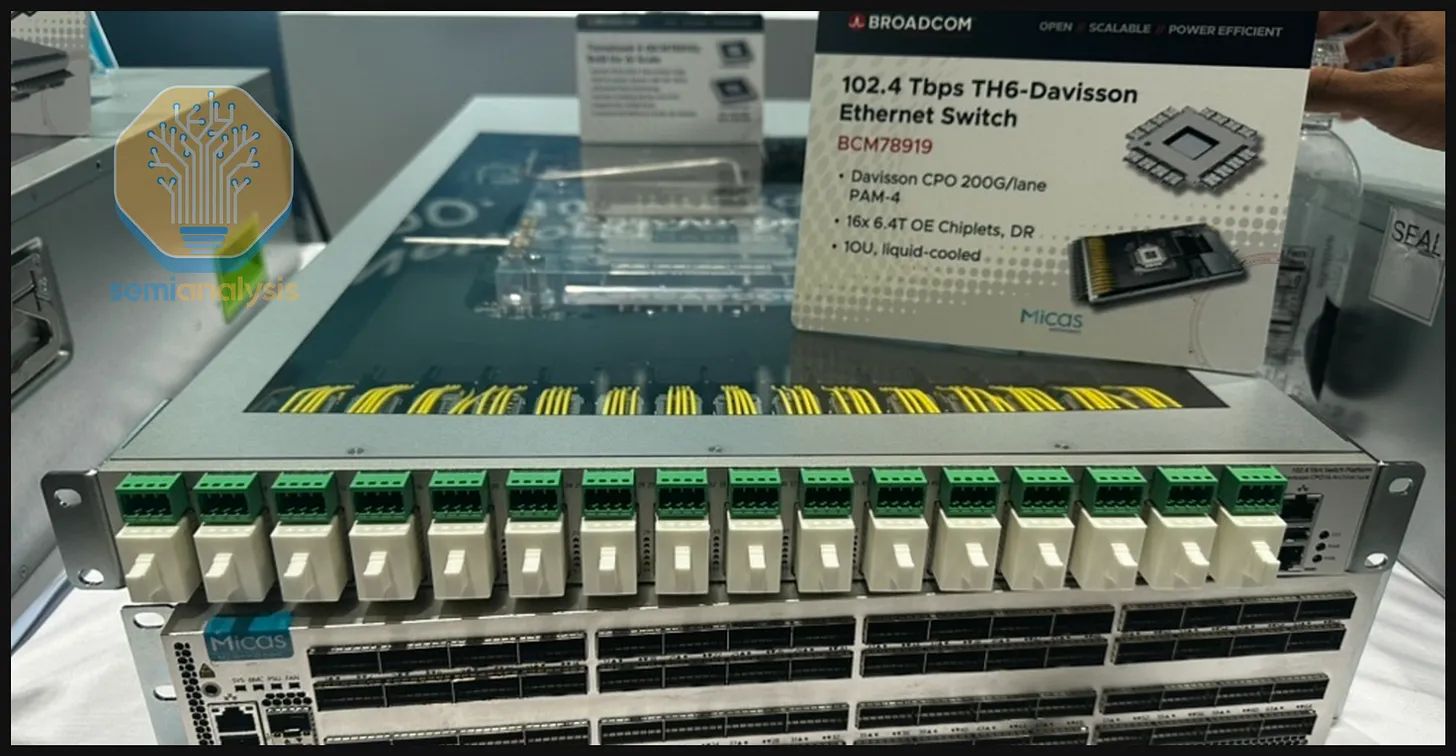
Unveiled in October 2025 and rolling out for deployment in 2025–2026, Davisson once again doubles bandwidth vs. Bailly to reach 102.4 Tbps.
| Spec | Davisson (TH6) |
|---|---|
| Switch ASIC | Tomahawk 6 (TSMC N3) |
| Aggregate bandwidth | 102.4 Tbps |
| Optical engines | 16 × 6.4T |
| SerDes speed | 200G / lane (up from 100G) |
| Optics | Davisson DR OE (200G / channel) |
| Port configurations | 128 × 800G or 64 × 1.6T |
| Packaging | Liquid-cooled, 10U chassis |
Key shift: 200G / lane SerDes
- The same generational leap Nvidia made on Quantum-X.
- Doubling lane speed reaches 102.4 Tbps without doubling fiber count.
- That said, in the FOWLP / TMV-based Bailly structure, 200G / lane is near the ceiling — the direct reason Broadcom needs to move the next generation to TSMC COUPE.
Open-ecosystem play
- Broadcom outsources box assembly to contract manufacturers (Micas, Celestica).
- Some customers like Japan's NTT are reportedly exploring buying Broadcom switch silicon and building proprietary CPO systems with their own OEs on top.
- That's a far more open-vendor approach than Nvidia's vertically integrated model.
Davisson implications
- Davisson is Broadcom's "mature production CPO" stage.
- It's the first generation that combines 200G / lane + TSMC N3 + a multi-vendor box ecosystem all at once.
- It's also close to FOWLP's last generation. The next generation flips the stack itself to TSMC COUPE.
4) Beachfront vs. Oceanfront — a fan-out approach toward scale-up
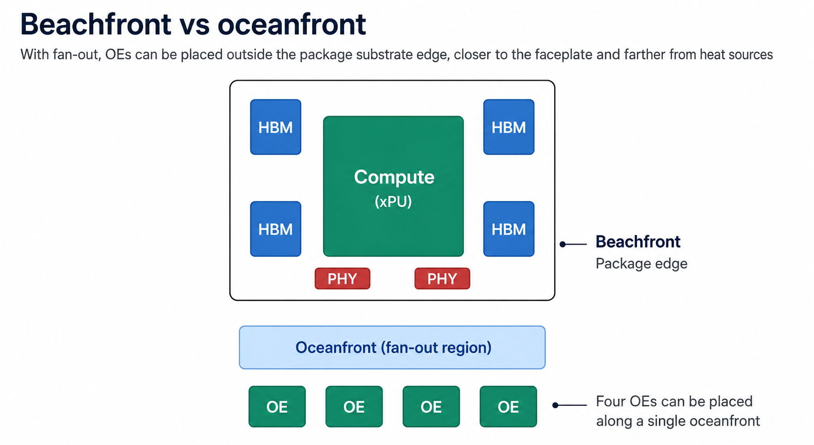
The architectural approach Broadcom is pushing to bond CPO onto customer ASICs (XPUs / GPUs) is a fan-out-based "beachfront vs. oceanfront" structure.
- Metaphor:
- "Beachfront" is the package substrate edge — limited shoreline.
- "Oceanfront" is the fan-out region extended beyond it, creating additional space to attach optical engines.
- Why it matters for scale-up:
- Pushing OEs farther from a hot xPU reduces the thermal stress on temperature-sensitive optics.
- OEs can be attached at the very last step of the assembly process → only known-good OEs touch the package, dramatically lifting yield.
- Four OEs can be lined up along a single oceanfront edge → today, 51.2 Tbps offload from a single edge.
- Roadmap trajectory (per Broadcom roadmap slides):
- 2025: 12.8 Tbps per oceanfront (1 OE)
- 2027: 51.2 Tbps per oceanfront (2 OEs)
- 2028: 102.4 Tbps per oceanfront (4 OEs)
- The CoWoS-S → CoWoS-L transition unlocks substrate edges greater than 100 mm, accommodating larger OE arrays.
5) Strategic positioning
- The customer-ASIC business is the real prize.
- Broadcom isn't simply a switch vendor. It sits in the seat designing hyperscalers' custom ASICs.
- The production experience accumulated in CPO makes Broadcom a natural design partner the moment those customers want to bond CPO onto their own AI ASICs.
| Customer | Adoption stance |
|---|---|
| OpenAI | Picked Broadcom for the ASIC partnership. CPO experience is one of the core factors. |
| The most hesitant hyperscaler. Negative on CPO adoption due to reliability concerns, even though it's Broadcom's largest ASIC customer. | |
| NTT, etc. | Reportedly exploring buying Broadcom switch silicon and building proprietary CPO systems with their own OEs on top. |
- The Google paradox is worth flagging. Google relies on Broadcom for custom TPU silicon but rejects CPO deployment.
- Its infrastructure philosophy prioritizes reliability over peak performance.
- CPO's blast radius (one OE failure → 64+ ports lost) clashes with Google's operations model.
- A strong signal that even within the deepest customer relationship, CPO adoption isn't universal — it's workload-specific.
6) The pivot to the TSMC COUPE platform
Even Broadcom — the vendor with the most production experience — is moving its next-generation product to the TSMC COUPE platform. That means fundamentally revising some of the existing design decisions.
| Component | Existing Broadcom approach | COUPE approach |
|---|---|---|
| Packaging | FOWLP via SPIL | TSMC SoIC hybrid bonding |
| Coupling | Edge coupling | Grating coupling |
| Modulator | MZM | MRM |
| Speed ceiling | 100G / lane (TMV parasitics) | 200G / lane and beyond |
- Why the change?
- FOWLP can't push beyond 100G / lane because of TMV parasitics.
- Edge coupling doesn't fit cleanly with structures that put the OE on an interposer.
- As long as the existing approach holds, Broadcom falls permanently behind on the speed roadmap.
- The cost: even as the most production-experienced vendor, the IP accumulated in MZM / FOWLP doesn't transfer cleanly to MRM / SoIC. In effect, the design in the core area has to start over.
- The bet: the design support and tooling TSMC provides (PDK, EDA workflow, reference designs) offset the reset cost, and the long-term performance ceiling justifies the short-term pain. It's a strong signal of TSMC's leverage inside the CPO ecosystem — even the most experienced CPO vendor is committing to the TSMC platform.
7) Bottom line
Broadcom's Humboldt → Bailly → Davisson three-generation arc has built the most mature portfolio in production CPO. Each generation left a clear lesson.
- Humboldt proved CPO works in a real Ethernet switch but exposed SiGe's power penalty.
- Bailly transitioned to all-optical with a CMOS EIC and validated FOWLP at scale, but ran into the 100G / lane ceiling.
- Davisson doubles bandwidth via 200G / lane and TSMC N3, and it kicks off an open-ecosystem play through box-maker partnerships and a silicon-only sales channel.
The future is split.
- Broadcom continues its leadership in scale-out switches with Davisson,
- but the larger opportunity is scale-up CPO bonded inside customer AI ASICs — the beachfront / oceanfront fan-out approach is the on-ramp.
- The TSMC COUPE pivot is a signal that "even the most experienced CPO vendor finds it hard to out-engineer the TSMC manufacturing platform."
- In the end, the future of CPO isn't defined by who carries the most legacy CPO IP — it's defined by whoever masters the TSMC stack first.
(3) Nvidia's generation-by-generation CPO adoption timeline
This isn't a one-off 2026 event but a multi-year roadmap in which Nvidia, generation after generation, pushes CPO into deeper layers.
| Generation | Timing | CPO adoption surface | What it means |
|---|---|---|---|
| Quantum-X / Spectrum-X | 2H25–2H26 | Scale-out switch (back-end network) | First production CPO — supply-chain validation phase |
| Rubin | 2H26+ | Full-scale scale-out CPO deployment | Begins shifting some scale-out traffic from optical transceivers to CPO |
| Rubin Ultra | 2H27 | Phase 1 scale-up CPO — rack-to-rack | Pod-level domains like NVL576 / NVL1152 connect over fiber. Just the copper → optical swap delivers ~3–4× performance per unit of traffic. |
| Feynman | 2H28+ | Phase 2 scale-up CPO — intra-rack | Past 400G per lane, copper hits its limit even inside the rack. Optics fills intra-rack, rack-to-rack, spine, and DCI. Optical-lane demand jumps ~10×. |
- Nvidia chose a conservative path: start with the "least sensitive" surface and expand inward toward the most sensitive surface near the GPU as the supply chain matures.
- The follow-the-leader pattern, with Broadcom and the ASIC camp trailing Nvidia by 6–12 months, holds.
(4) Composite implications
- Nvidia and Broadcom converge on the same platform (TSMC COUPE), but their entry paths are opposite.
- Nvidia enters via a vertically integrated end-to-end system (switch + OE + ELS + fiber routing + cassette) — fast adoption is possible, but customer lock-in grows.
- Broadcom builds a more open ecosystem via bare die + contract manufacturer + customer-ASIC partnerships — adoption pace is slower but fits a multi-vendor world better.
- Across both, 200G / lane + an MRM-class modulator + hybrid bonding is settling in as the production CPO baseline.
- That said, both vendors are in a market-validation phase rather than mass adoption. Quantum-X uses detachable sub-assemblies; Bailly / Davisson run without multi-OE redundancy; neither has yet reached an architecture that recovers cleanly when one OE fails in the field.
- So the 2026 CPO market is shaped less by "who builds the fastest OE" and more by "who can transplant the serviceability and multi-vendor ecosystem of pluggables onto CPO fastest."
Link resiliency — the hyperscaler value beyond power saving
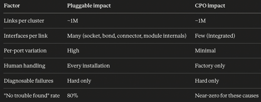
- CPO's stability story isn't a single dramatic improvement — it's a system-level removal of the variables that produce soft failures: fewer interfaces, tighter tolerance management, more uniform ports, and the elimination of human-touch steps.
- In large AI clusters, link resiliency isn't a nice-to-have — it ties directly to the useful training time you can extract from the fleet.
- A dead link halts training for a GPU group or drops throughput as routing detours; at the scale of tens of millions of GPU-hours, even sub-percent differences in link uptime translate into real losses.
- CPO replaces a still-disorganized, hand-touched optical supply chain with a more systematized, predictable, factory-sealed structure.
- That's why some hyperscalers say "CPO's biggest value isn't power saving — it's resiliency."
- One caveat: CPO's blast radius grows. A single OE failure can affect 64+ ports, so whether CPO's resiliency model can be reliably detected, isolated, and recovered in real datacenter operating environments remains a separate, central challenge.