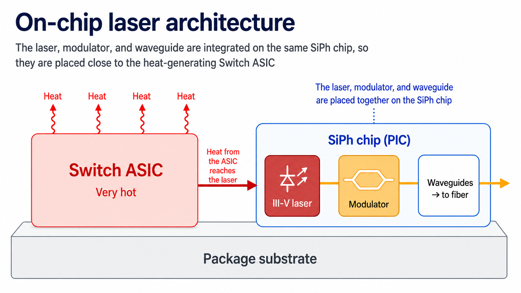
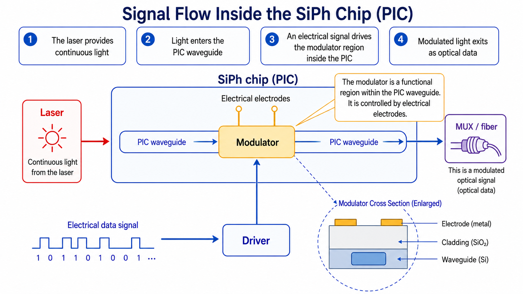
In CPO, the laser doesn't generate the data itself; it provides the source light that the modulator imprints information onto.
There are two main options.
Structure
Description
On-chip laser
III-V (InP; indium phosphide) laser material is bonded directly onto the silicon-photonics chip, integrating the laser inside the optical engine; laser, modulator, and waveguide live on the same die.
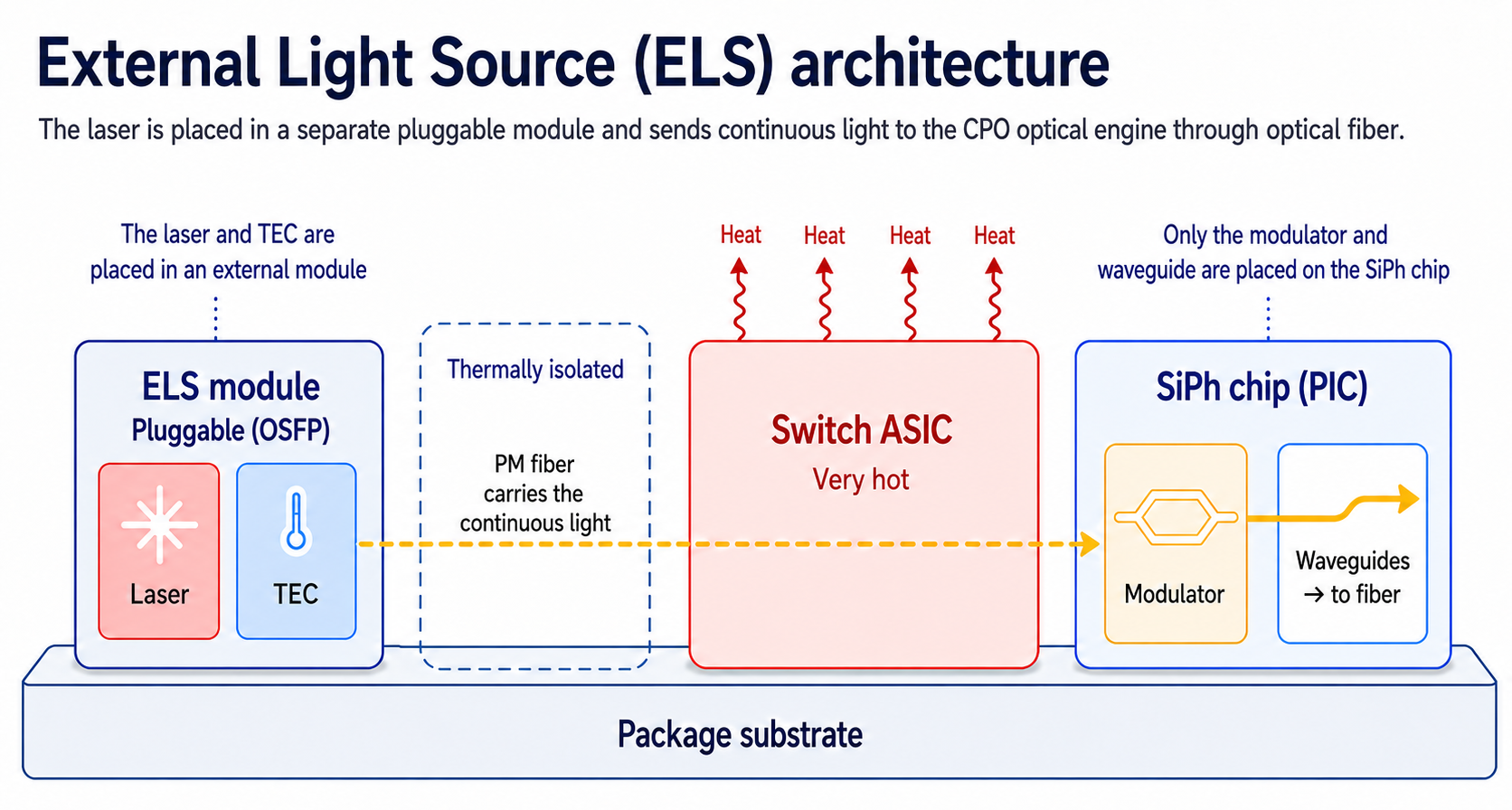
External Light Source (ELS)
The laser is separated into its own module (a pluggable transceiver, OSFP form factor, etc.), which feeds continuous light into the optical engine via fiber.
(1) On-chip laser
Structurally the simplest-looking choice.
Because laser, modulator, and waveguide live on the same die or inside the same optical engine, external optical connections shrink, and in theory insertion loss can be lowered.
But operational risk in real CPO deployment is high.
Risk
Why it matters
One laser failure can take the whole CPO engine down.
The on-chip laser's blast radius is 64+ ports — at 800G per port, a 64-port outage means losing 51.2 Tbps of fabric capacity.
Thermal sensitivity
The CPO optical engine sits right next to a high-thermal ASIC, and laser modules are heat-sensitive.
Output ceiling
An on-chip laser may not put out enough optical power to overcome system-level optical loss.
Maintenance constraints
Replacing one laser may require replacing the entire optical module.
So an on-chip laser carries significant risks on field operation, thermal reliability, and serviceability.
(2) ELS (External Light Source)
Unlike an on-chip laser sitting inside the optical engine, ELS pulls the laser out of the engine — light is generated in a separate laser module and supplied to the optical engine through fiber.
Industry consensus today aligns more with ELS than with on-chip lasers.
Item
Detail
What it means
Advantages
Field replacement is possible
If a laser module fails, only the ELS module needs swapping — no need to disassemble the optical engine.
Thermal isolation
The laser module is physically separated from the high-heat ASIC.
Easier high-power laser design
The laser module's temperature is decoupled from ASIC heat, making higher-output laser designs feasible.
Lower blast radius
Laser-module failure no longer translates directly into optical-engine failure.
Disadvantages
Relatively long optical path
An additional connector path from ELS module to optical engine adds optical loss.
High-power laser is mandatory
The laser has to put out more power to cover that added loss.
Power for ELS-module temperature control
The TEC (Thermoelectric Cooler) keeping the ELS module thermally controlled draws additional power.
Partially offsets CPO's power-saving premise
Even after lowering optical-engine power consumption, ELS module temperature control consumes additional power.
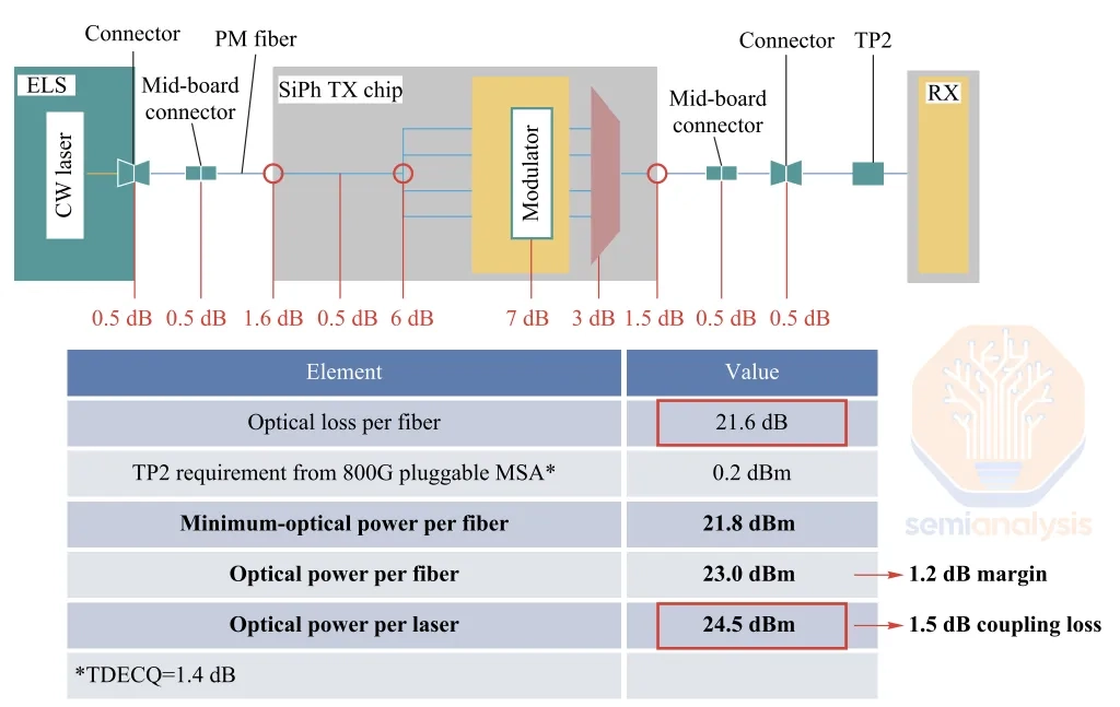
1) Why does ELS need a high-output laser?
ELS gains reliability and serviceability at the cost of a longer optical path that accumulates connector / coupling / modulation losses.
With ELS, total optical loss per fiber comes to 21.6 dB. Summing every optical-loss term in the diagram above yields 21.6 dB.
The minimum optical power required at TP2 (Test Point 2 — where optical-signal output and quality are checked, just before the RX) is 0.2 dBm,
so the minimum output the ELS module's CW (Continuous Wavelength) laser must produce is 21.6 dB + 0.2 dBm = 21.8 dBm,
adding 1.2 dB of additional margin lifts the input requirement at the optical fiber to 21.8 dBm + 1.2 dB = 23.0 dBm,
and adding the 1.5 dB coupling loss between laser and fiber pushes the laser-output requirement to 23.0 dBm + 1.5 dB = 24.5 dBm.
2) ELS as a double-edged sword
The CW laser inside the ELS module and the TEC that cools it together account for ~70% of ELS power consumption.
It is not as simple as "putting optics close to the XPU / ASIC reduces power."
CPO's power reduction comes from a shorter electrical path, low-power SerDes, and the option to remove or shrink DSP — but ELS introduces new burdens of optical loss and the additional laser and cooling power that loss requires.
(3) Nvidia's laser ecosystem
Vendor
Technology
Usage
Lumentum
Single high-output DFB laser (Distributed Feedback)
Used for stable single-wavelength source output.
Ayar Labs
DFB laser arrays
Multiple DFB lasers arranged in arrays produce source light covering a range of wavelengths.
Innolume
Quantum-dot mode-locked comb lasers
A comb-laser single module can output a wide range of wavelengths, useful for WDM networking systems — no need to procure many separate lasers.
Xscape, Enlightra, Iloomina
Pumped nonlinear resonant comb lasers
The fact that Nvidia is exploring multiple laser architectures simultaneously suggests that the laser source is not yet a standardized commodity but rather an important differentiation layer in CPO system design.
(4) Implications
The crux of CPO isn't just bonding the optical engine close to the XPU / ASIC. Where to place the laser, how much optical loss can be reduced, how to repair and absorb laser-module failure, and how to approach thermal management together determine system-level competitiveness.
On-chip laser is strong on integration efficiency; ELS is strong on reliability and serviceability. From the standpoint of current CPO deployment, ELS is the more realistic option, but at the cost of carrying laser-power and TEC-power burdens.
6. Modulator Comparison Inside CPO
Light from the laser, on its own, carries no data.
The modulator changes the intensity, phase, or absorption of the input laser to encode an electrical signal onto the optical carrier.
In CPO, the choice of modulator is not a simple component selection — it is a key variable that determines the entire structure of the optical engine.
Decision factor
What the modulator drives
Footprint
Determines how many channels can fit inside the optical engine.
Power
Affects per-bit energy efficiency and cooling burden.
Thermal sensitivity
Determines whether it operates stably next to the high-temperature XPU / ASIC.
WDM compatibility
Determines how efficiently many wavelengths can ride inside one fiber.
Signal cleanliness
Affects quality for advanced modulation like PAM4 or QAM.
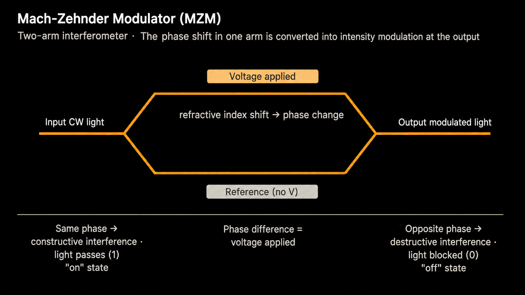
(1) Mach-Zehnder Modulator (MZM)
MZM splits incoming light into two waveguide arms and applies voltage to create a phase difference between the two paths.
When the two paths are recombined, the phase difference converts into intensity modulation, enabling data modulation.
Structural feature
Core strength
Core weakness
Two-arm interferometer
Signal cleanliness and linearity
Large footprint and high power consumption
Item
Detail
What it means
Advantages
Well-known structure
Lots of implementation experience and relatively low design risk.
Low thermal sensitivity
Performance variation with temperature is smaller than for MRM.
Strong linearity
Favorable for advanced modulation like PAM4 and QAM.
Strong for high-speed scaling
200G is proven, and 400G has been mentioned as feasible.
Disadvantages
Footprint is very large (~12,000 µm² due to its two waveguides and electrode structure)
Hard to fit many channels inside the optical engine.
High power consumption
Can conflict with CPO's power-efficiency goals.
Disadvantageous for WDM density
Area burden grows as channel count rises.
MZM suits architectures that prioritize raw bandwidth and signal quality.
That said, the footprint burden is heavy in environments like CPO where fiber count and package area are constrained.
Scale-up CPO startups like Nubis taking the MZM path do so because they prioritize signal quality and bandwidth.
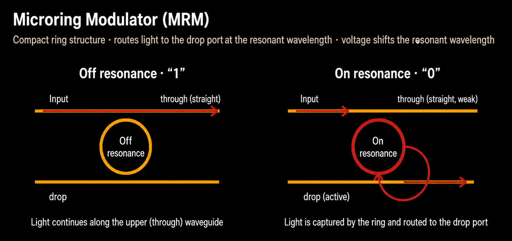
(2) Micro-Ring Modulator (MRM)
The MRM is a modulator that uses a ring-shaped waveguide as a "wavelength-selective gate."
Resonance occurs only at specific wavelengths inside the ring.
When the input light's wavelength matches the ring's resonance wavelength, light couples strongly into the ring.
At that moment the light cannot just pass through the straight waveguide — it bleeds out the drop port, or the through-port intensity drops.
Applying voltage shifts the ring's refractive index, which shifts its resonance wavelength.
In other words, voltage rapidly toggles the ring between "in resonance / out of resonance," modulating the output light's intensity between 1 and 0.
Structural feature
Core strengths
Core weakness
Resonant ring
Very small footprint, relatively low power consumption, and good fit with WDM
Thermal sensitivity
Item
Detail
What it means
Advantages
Very small footprint (25–225 µm²)
Roughly 50–500× smaller than MZM. Many channels can fit inside the optical engine.
Native WDM support
Rings can be placed per wavelength.
Low power per bit
Favorable for CPO's power efficiency goals.
Can absorb part of the mux / demux function
Because each ring acts like a resonant filter responding only to a specific wavelength, it can filter only its own wavelength channel — internalizing part of the wavelength-selection function that mux / demux normally provides.
Disadvantages
Very thermally sensitive
10–100× more sensitive than MZM / EAM. Even small temperature shifts move the resonance.
Active thermal control may be required
Non-linearity issues
Signal-quality burden grows for higher-order modulation like PAM4 / 6 / 8.
MRM is the strongest density / WDM option in CPO.
The thermal-control burden is heavy, but in environments where the optical engine can fit only a limited number of fibers, the small footprint and native WDM support are major advantages.
That's why Nvidia, TSMC COUPE, Ayar Labs, Lightmatter, Ranovus, and others have either chosen the MRM path or remain compatible with it.
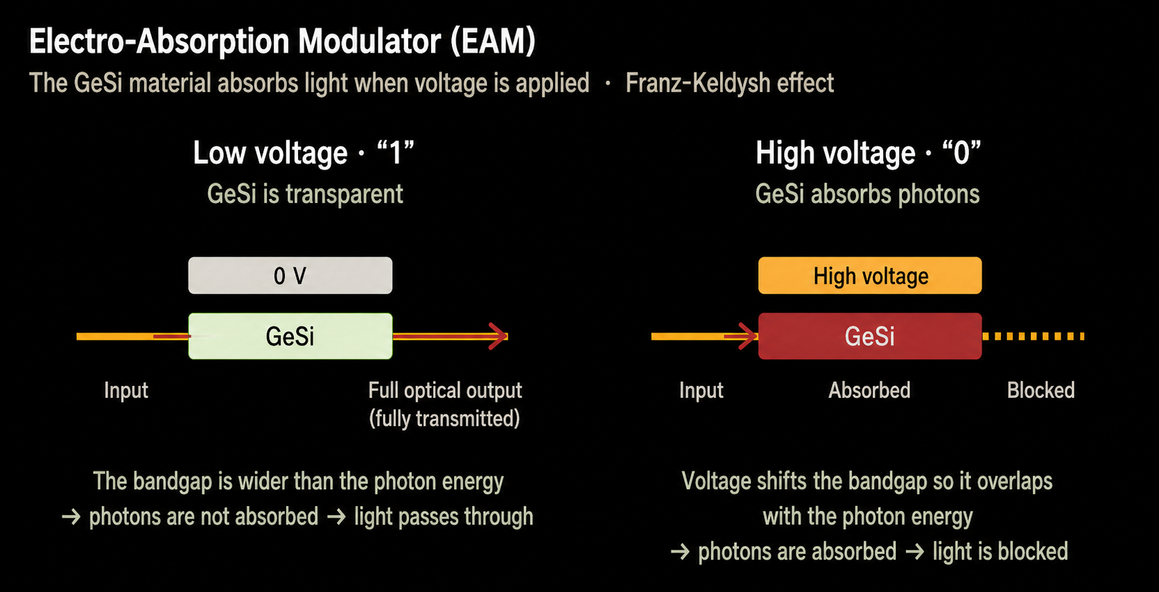
(3) Electro-Absorption Modulator (EAM)
Voltage is applied to change the absorption properties of GeSi (Germanium-Silicon), encoding data by either passing or absorbing the light.
Unlike MZM (which uses phase interference) or MRM (which uses resonance), EAM directly modulates the material's absorption property.
Structural feature
Core strengths
Core weakness
Voltage-controlled absorption
Thermal stability, compact footprint
No WDM support
Item
Detail
What it means
Advantages
Strong thermal stability
Can be more stable than MRM in hot packaging environments.
Compact footprint (~250 µm²)
Far more compact than MZM (~12,000 µm²).
Lower power consumption than MZM
Better than MZM on power efficiency.
Suitable for placement near the high-thermal XPU / ASIC
Applicable in structures that are thermally challenging.
Disadvantages
GeSi stability concerns
Long-term material stability of GeSi needs further validation.
No native WDM support
Doesn't provide the wavelength-selective gating MRM does.
The native band edge (the wavelength range where GeSi naturally begins to absorb light) is centered on C-band (~1530 nm), so it's easy to make GeSi switch between absorption / transmission with voltage in that band. It does not align with the datacom standard O-band (1310 nm).
May not align with the existing datacom optics supply chain.
Requires a separate multiplexer
Implementing WDM adds extra optical components and insertion loss.
EAM is closer to "a compact modulator that operates stably in hot environments" than to "the densest WDM architecture."
In architectures where the modulator is placed near or under a hot XPU / ASIC, like Celestial AI's, EAM can be a sensible choice.
(4) Comparison
1) Side by side
Property
MZM
MRM
EAM
Footprint
~12,000 µm²
25–225 µm²
~250 µm²
Power per bit
High
Low
Medium
Thermal sensitivity
Low
Very high
Low
Native WDM support
No
Yes
No
Linearity
Excellent
Poor
Good
Max bandwidth
200G+
100–200G
100–200G
Insertion loss
3–5 dB
3–5 dB
4–5 dB
Industry adoption
Relatively small (niche), Nubis
Dominant, Nvidia / TSMC / startups
Relatively small (niche), Celestial AI
2) By architecture priority
Architecture priority
Better-fit modulator
Why
High signal quality / linearity
MZM
Strong linearity and good for advanced modulation.
High channel density / WDM efficiency
MRM
Very small and native WDM support.
Hot-package robustness
EAM
Low thermal sensitivity and compact footprint.
Lowest power per bit
MRM
Small capacitance and compact footprint help energy efficiency.
Simple WDM scaling
MRM
Ring resonance can be used as a wavelength-selective element.
When you don't want to worry too much about thermal control
MZM or EAM
Less sensitive to temperature swings than MRM.
(5) Implications
The reason Nvidia and TSMC picked MRM isn't simply that the modulator's performance is superior;
It's because CPO's core bottleneck is fiber density and package density.
MRM is thermally sensitive, but its very small footprint and native WDM support directly address CPO's fiber-economy problem.
7. The Optical-Engine (OE) Scaling Roadmap
OE scaling in CPO isn't a single-bottleneck problem; it's pushing three scaling vectors simultaneously — fibers × speed × wavelengths.
Today's CPO OEs start in the 1.6T–3.2T aggregate-bandwidth range, but for CPO to justify its complexity vs. modular optical transceivers, OE density needs to climb several times higher.
(1) Where OEs stand today
Vendor / Engine
Bandwidth
Device form-factor notes
Nvidia Quantum CPO
1.6T
Compact form factor; first volume product.
Nvidia Spectrum CPO
3.2T (planned)
Compact form factor; second-gen target product.
Broadcom Bailly
6.4T
Two to three times wider; requires two FAUs.
Marvell
6.4T
Large footprint, requires two FAUs, no production-system plan.
Nvidia's 3.2T Spectrum-X photonics switch is a CPO architecture but is not yet a stage where it shows an overwhelming shoreline-bandwidth-density advantage vs. pluggables + LR SerDes.
The NVIDIA 3.2T OE is "optics placed close" — not "shoreline made denser." 3.2T is still driven by 16×200G SerDes, so the lane-escape count required at the package edge isn't very different from a transceiver setup. Today's advantage is more about electrical loss / power / signal integrity than density.
So CPO's next milestone is not "an OE that works" but "a much higher-density OE."
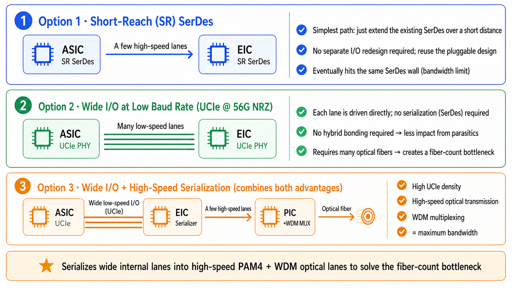
(2) Three approaches to the host-ASIC ⟷ OE-EIC interface
Option
Structure
Strengths
Limits
Option 1: Short-reach SerDes
Keeps the existing SerDes architecture but shortens reach.
Easy migration; reuses existing designs.
Eventually hits the same SerDes wall.
Option 2: Wide low-speed lanes / UCIe
Many low-speed lanes connect to the EIC in parallel.
EIC simplifies; hybrid-bonding burden eases.
Each fiber must be driven directly, blowing up fiber count.
Option 3: Wide I / O + serialization
Internally thousands of slow lanes; externally serialized to 200G+ optical lanes.
Highest performance potential.
Most complex; high packaging / EIC design difficulty.
Option 1 is the most realistic short-term migration path,
Option 2 simplifies the electrical side but pushes the fiber-attach burden onto the optical / mechanical side,
Option 3 is closer to the long-term architecture for CPO to deliver real bandwidth-density advantage.
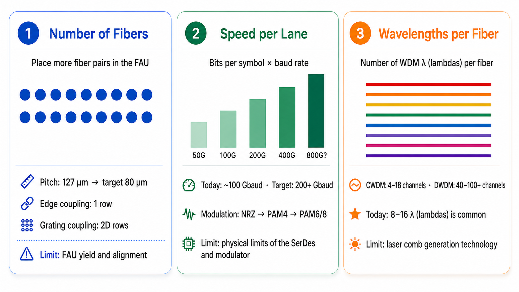
(3) The three factors of optical-bandwidth scaling
Total OE bandwidth = number of fibers × speed per lane × wavelengths per fiber.
To raise OE bandwidth, you have to:
increase the number of fibers attached to the FAU,
increase per-lane speed, or
increase the number of wavelengths riding on each fiber.
Vector
Meaning
Bottleneck
Number of fibers
The number of fibers physically attachable to the OE.
Fiber count is bounded by fiber pitch. Today's pitch sits at ~127 µm, with a target of 80 µm. Higher fiber counts increase alignment complexity and manufacturing-yield risk.
Per-lane speed is being pushed from 100 Gbaud to 200 Gbaud, with modulation moving NRZ → PAM4 → PAM6 / 8.
Higher-order modulation lets you carry more bits without raising symbol rate, but reading those bits accurately requires a much cleaner signal.
PAM4 carries 1 symbol = 2 bits across four voltage levels (e.g. 00, 01, 10, 11);
The denser the levels in the same voltage budget (PAM4's ~0.33 V gap → PAM8's ~0.14 V gap), the more even small noise smears one level into the next.
The fight stops being one against the wire's speed limit and becomes one against the noise floor — the same physical limit on lossy copper paths that capped 244 Gbaud also makes PAM8 decoding harder.
As lane speed rises:
SerDes has to send and receive cleaner, faster electrical signals.
The modulator has to respond fast enough.
Optical / electrical bandwidth approaches its limits.
Signal loss and noise increase.
PAM4 / PAM6 / PAM8 demand higher linearity and SNR.
Equalization and DSP get harder.
Power consumption rises.
For wavelengths per fiber, DWDM (Dense WDM), comb lasers, and 16λ / 64λ sources (capable of carrying 16–64 wavelengths internally) become the key levers.
A side note: the structure of WDM and what it means in CPO
WDM (Wavelength Division Multiplexing) sends multiple wavelengths — different "colors" of light — through a single fiber simultaneously. Each wavelength carries an independent data stream, raising bandwidth per fiber without raising fiber count.
Element
Role
Multiple lasers / comb source
Generate optical carriers at different wavelengths.
Modulator
Imprint data onto the light at each wavelength.
MUX
Combine many wavelengths into a single beam over one fiber.
Single fiber
Multiple wavelengths travel together through one fiber.
DEMUX
At the receiver, light is separated by wavelength.
Photodetector (PD)
Each wavelength's light is converted into electrical signal.
WDM's two main flavors:
Type
Channel spacing
Channel count
Use cases
CWDM (Coarse WDM)
~20 nm
4–18 channels
Lower-density, simpler optical networking; thermal management is comparatively easy.
DWDM (Dense WDM)
< 1 nm
40, 80, 100+ channels
High-density, complex optical networking; precise wavelength control is required.
Why WDM matters in CPO:
Fiber bandwidth = fiber count × wavelengths per fiber × data rate per wavelength.
CPO is ultimately limited in how many fibers it can attach. Even with 2D fiber arrays via grating coupling, you can't connect indefinitely many fibers.
So in CPO, "loading more bandwidth onto each fiber" matters more than "attaching more fibers."
The fiber count one optical engine can attach is bounded.
Each optical port has to handle as much bandwidth as possible.
Per-lane SerDes speed at 200G or 400G runs into growing physical burdens.
The remaining lever is wavelengths per fiber.
For example, putting 8 wavelengths on each fiber multiplies bandwidth per fiber by 8× without raising fiber count.
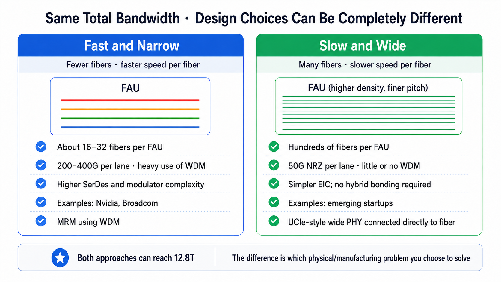
(4) Fast & Narrow vs. Slow & Wide
Architecture
Description
Representative direction
Core bottleneck
Fast & Narrow
Few fibers, high per-lane speed, and WDM
Nvidia, Broadcom-style
SerDes, modulator, WDM control
Slow & Wide
Many fibers, each running at low speed
Wide-and-slow architecture
FAU throughput, fiber-attach yield
Fast & Narrow leans on WDM and high-speed modulation to reduce fiber count.
Slow & Wide lowers optical / electrical-speed burden but creates a manufacturing problem of attaching hundreds of fibers.
If CPO's practical bottleneck is FAU yield, Fast & Narrow is the more scalable direction.
(5) Bandwidth-scaling scenarios
Approach
Fibers
Speed
λ / fiber
Total OE BW
Density
1: MRM 50G NRZ baseline
9
50G
1
0.2T
0.2 Tbps / mm
2: MRM 50G + 16λ WDM
18
50G
16
6.4T
6.4 Tbps / mm
3. ==MRM 200G PAM4 + 8λ WDM==
==18==
==200G==
==8==
==12.8T==
==12.8 Tbps / mm==
4. MRM 200G + 16λ + 2 fiber rows
36
200G
8
25.6T
25.6 Tbps / mm
5. MZM 400G PAM4, 8 fiber rows
128
400G
1
22.8T
11.2 Tbps / mm
12.8T is the inflection point for OE scaling.
The same 12.8T bandwidth can be reached via multiple paths.
MRM + 200G PAM4 + 8λ WDM
Pushes per-lane speed to 200G,
carries 8 wavelengths per fiber,
and reaches 12.8T with relatively few fibers.
MRM + 50G + 16λ WDM
Keeps per-lane speed low,
raises wavelengths per fiber to 16λ,
and scales bandwidth via WDM density.
MZM + very high fiber count
Raises bandwidth via fiber count instead of WDM,
which means significantly more fibers and FAU capacity.
MRM + WDM can reach 12.8T with about 18 fibers, while MZM-based approaches need ~128 fibers for similar bandwidth.
So MRM + WDM is attractive on fiber economy and FAU yield. With the same bandwidth at fewer fibers, the burdens on fiber pitch, alignment complexity, FAU assembly yield, and packaging footprint all drop sharply.
Combining all available technologies, bandwidth up to 25.6T becomes feasible — option 4, which doubles the fiber count of option 3.
(6) The CPO adoption process and its limits
CPO adoption is bottlenecked more by deployment friction than by technical feasibility.
Initial products are arriving, but 2026 is closer to a market test of supply chain, reliability, and customer education than mass adoption.
1) Nvidia's early adoption timeline
Product
Use case
Availability
Quantum CPO
InfiniBand back-end scale-out
2H 2025
Spectrum CPO
Ethernet scale-out
2H 2026
2026 expected volume is given as 10–15k units — closer in character to early deployment / market validation than to a wholesale replacement of optical transceivers.
2) The biggest customer concerns about CPO
Concern
Optical transceivers
CPO
Interoperability
Multi-vendor module ecosystem exists
No standard yet; vendor-proprietary form factors dominate
Serviceability
Front-panel hot-swap available
Chassis open, FAU detach, fiber disturbance (a single component repair requires disassembling the entire module)
Supply chain
Vendor competition exists
Possible lock-in to a specific vendor ecosystem
Repair time
Module-swap centric
Burdens of optical alignment and chassis-level repair
The biggest customer concerns about CPO are the lack of interoperability and serviceability.
Optical transceivers spread thanks to a cross-vendor standards stack, but CPO is closer to a "wild west" phase where each vendor is pushing its own proprietary system.
3) What CPO interoperability requires
Layer
Why it matters
Electrical
The CPO module has to be compatible with the latest SerDes / ASIC interfaces.
Optical
Optical-level cross-compatibility with other transceiver types in the cluster.
Mechanical
Required to enable detachable / replaceable OEs.
CPO standardization needs electrical interface, optical signaling, and mechanical form factor to all line up before a vendor-agnostic ecosystem becomes possible.
4) Why are vendors pushing end-to-end solutions?
It's hard for customers to assemble individual CPO components themselves.
Inside a dense chassis, fiber management, front-plate density, modulator architecture, ELS integration, and FAU alignment are all entangled.
That's why early CPO requires vendors like Nvidia to offer a full system bundling switch + OE + ELS + fiber routing + cassette.
It's the realistic way to start adoption, but it also amplifies customer lock-in and interoperability problems.
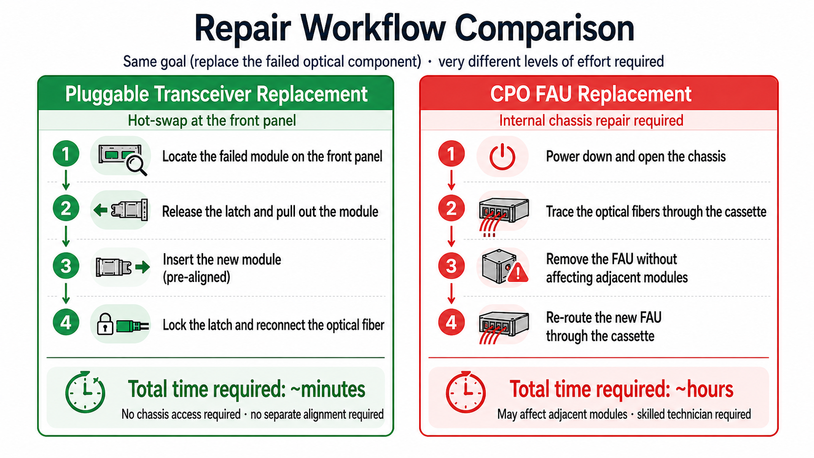
5) The CPO repair problem
Repair flow: optical transceivers vs. CPO
Optical components are more environmentally sensitive than copper
Sensitivity factor
Effect
Temperature
Wavelength shifts, efficiency degradation, growing need for TEC
Aging
Photonic-component efficiency degrades over time
Contamination
A single dust particle on the fiber tip can dramatically increase insertion loss
Humidity
Affects sensitive optical interfaces
Mechanical shock / physical deformation
Causes fiber bending, breakage, and signal degradation
Copper wires can keep functioning even with minor damage,
whereas fiber-end contamination or micron-level misalignment translates directly into link loss.
So CPO serviceability isn't simply a module-replacement problem — it's a precision optical-handling problem.
(7) Implications
CPO has lab-level reliability advantages and density / power benefits, but two structural hurdles need to clear before mass adoption.
Barrier
Meaning
Interoperability
Has to move from a proprietary ecosystem to a standardized multi-vendor ecosystem
Serviceability
Chassis-level optical repair has to come down to a field-operable form
For hyperscalers, CPO can be an acceptable trade-off.
The benefits on power, density, and SerDes scaling are meaningful enough.
For mass deployment more broadly, however, interoperability and serviceability remain unresolved bottlenecks.
That's why a 2026 deployment volume of 10–15k units fits the "market test" framing.