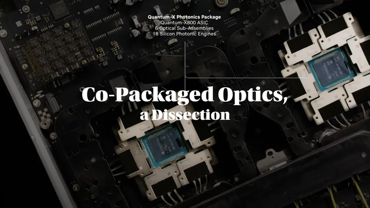
On CPO Pt. 5 | OCS, Testing, and the Optical Value Chain
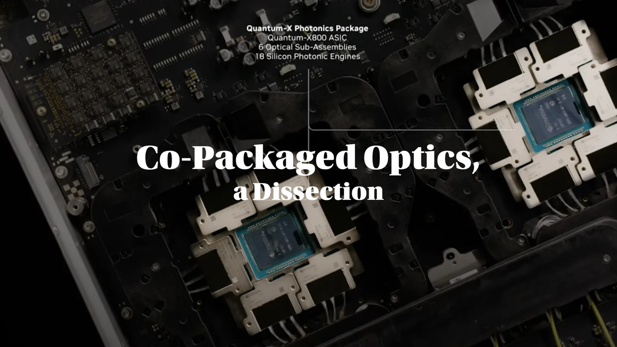
OCS — another optical trend that runs orthogonal to and alongside CPO; testing as a critical-path bottleneck in the CPO era; and an end-to-end view of the optical value chain from wafer → laser → PIC → transceiver.
On CPO
- Part 1, The Phased Transition from Pluggables to CPO
- Part 2, The Economic and Architectural Case for CPO
- Part 3, Inside the Optical Engine
- Part 4, Today's Major CPO Products
- Part 5, OCS, Testing, and the Optical Value Chain
9. OCS (Optical Circuit Switching)
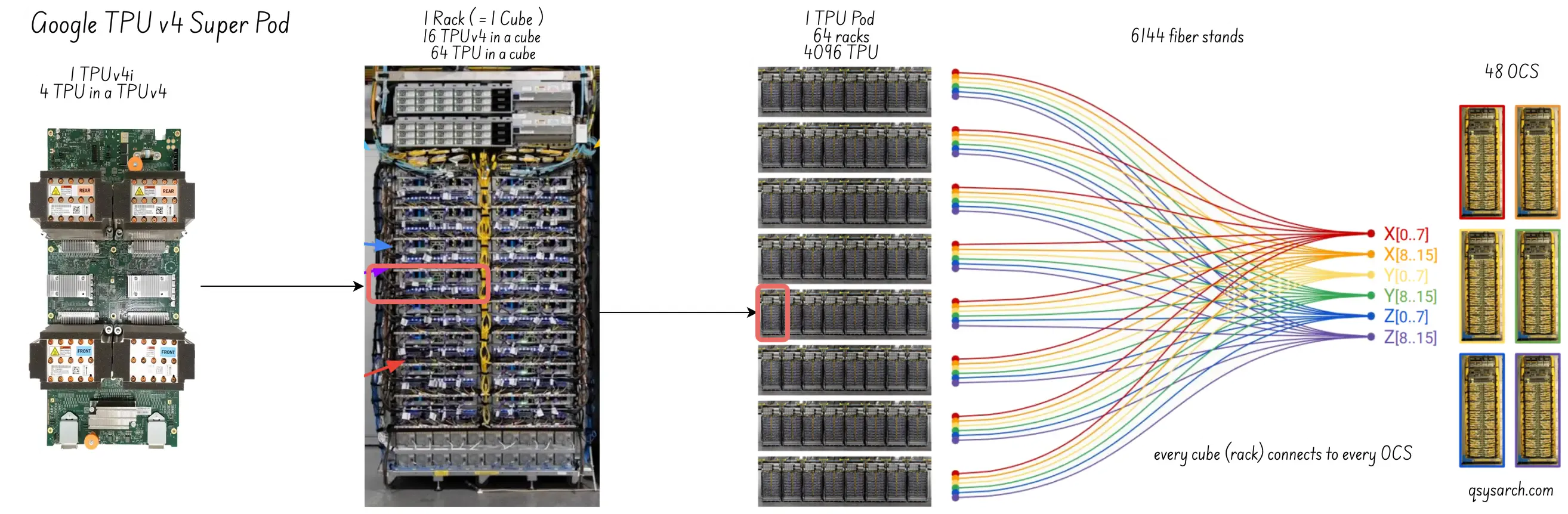
- OCS is another optical trend running orthogonal to and alongside CPO.
- It steers light directly with mirrors instead of converting it to electrical signals, removing one round of the optical → electrical → optical conversion that traditional optical networking requires.
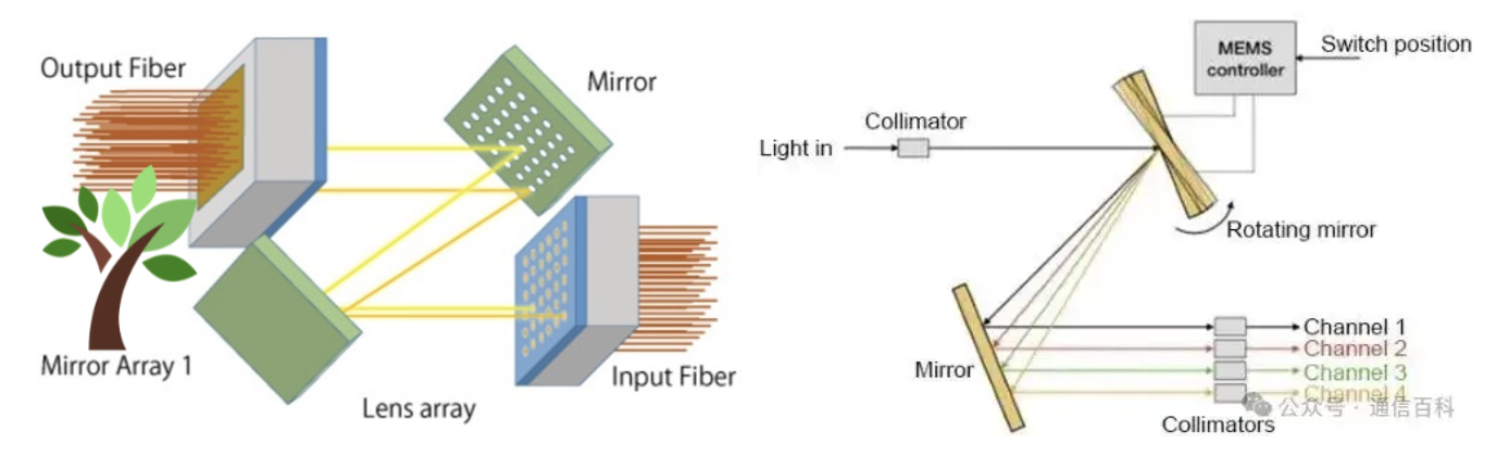
(1) How it works
- Instead of routing traffic between two endpoints through multiple layers of packet switches, OCS creates a direct optical path between them.
- Reducing electrical ↔ optical conversions cuts power and latency dramatically, lowers switching overhead, and makes fabric configuration more flexible.
- That said, OCS does not switch packets directly — rather than processing the traffic itself, it functions as a new networking layer that changes the path the traffic travels along. So it doesn't replace the existing packet switches; it adds a layer above them.
(2) Two technology roadmaps
| Vendor | Technology | Characteristics |
|---|---|---|
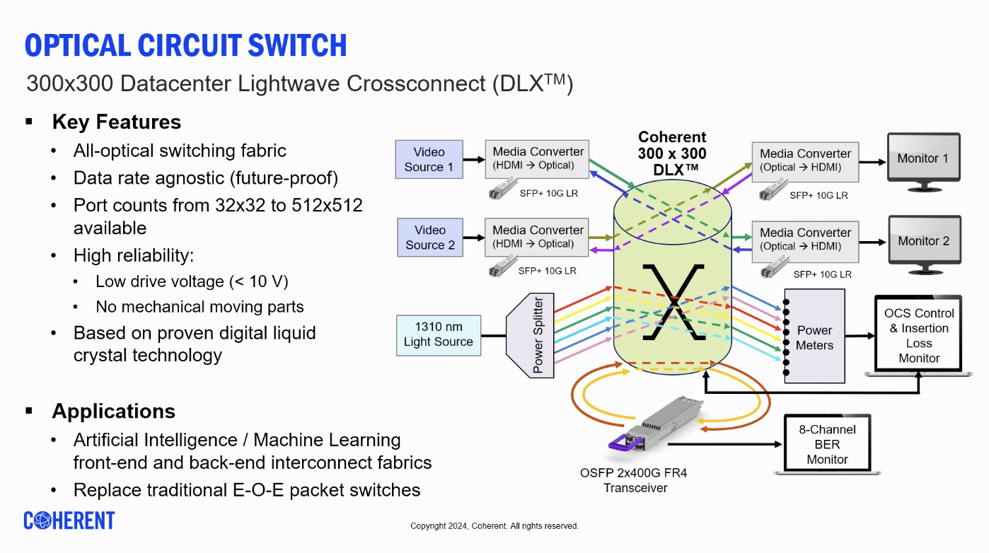
| Lumentum + Google | MEMS | Combines precision, reliability, and cost efficiency; adopted in Google TPU, accounting for 8–10% of TPU BoM |
| Coherent | LCOS (Liquid Crystal on Silicon) | Long-validated technology in telecom, no moving parts so reliability is high; 2–4× more expensive than MEMS |
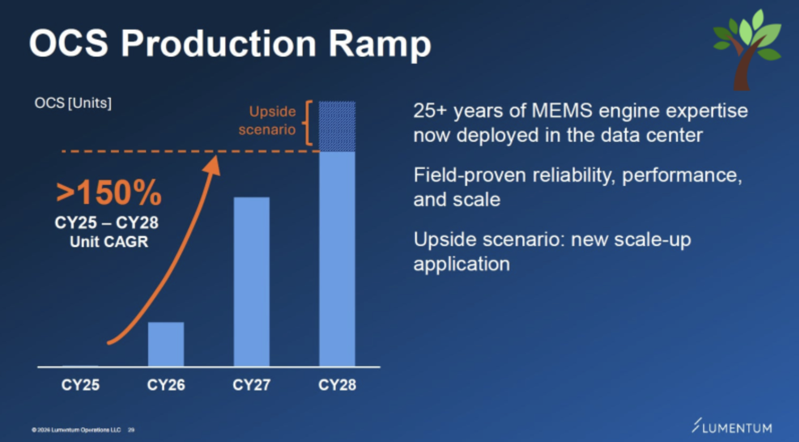
- At OFC 2026 Lumentum announced it had signed a "new multi-year, multi-billion-dollar OCS agreement." Given that FY25 revenue was $2.1B, OCS alone is essentially adding the equivalent of one year's revenue as a new line.
- In its 1Q26 update, Lumentum guided to CY27 OCS ARR of $1B+, with CY25–CY28 OCS demand expected to grow at >150% CAGR (on a scale-out-only scenario excluding Google TPU).
- Three hyperscalers are currently adopting Lumentum OCS, with two of them carrying the majority of volume.
- On the supply side, Lumentum had been 100% in-house production, but in its 1Q26 earnings call it confirmed it is shifting to scaling via contract manufacturers to absorb the demand surge — a structure that lifts revenue and margin together by improving efficiency through higher common-component output.
(3) Where it's being adopted
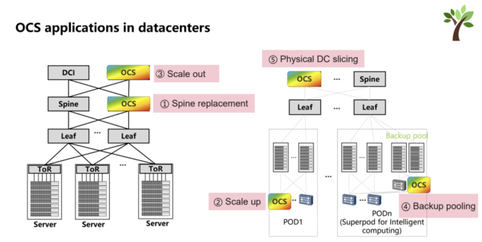
- Potential to expand into spine-switch replacement in new datacenters, TPU interconnect, and intra-rack scale-up applications.
- In some use cases, OCS can replace existing copper-based switches.
(4) OCS expands optical-transceiver demand
- Once OCS mirrors are deployed, you can keep reusing them while only swapping transceivers — plug in 800G and you have an 800G switch; plug in 1.6T and you have a 1.6T switch.
- So adopting OCS isn't a transceiver replacement — it adds connection points.
- Because the application is more sensitive to transceiver performance, the trend favors top-tier optical-transceiver vendors.
(5) Implications
- OCS is not a CPO competitor — it's another optical trend orthogonal to CPO.
- If CPO shrinks the electrical path at the device level, OCS shrinks the count of optical-electrical conversions at the fabric level.
- Both work to lift long-term transceiver demand, and they're two parallel axes hyperscalers are pushing simultaneously.
10. The Importance of Testing
- As optics moves closer to the chip — Pluggables → LPO → NPO → CPO — the cost of an optical-engine failure keeps rising, because "package-level scrap" replaces "module replacement" as the default failure mode.
- In the CPO era, testing isn't simple back-end QA — it becomes a critical-path enabler of CPO adoption.
(1) Why testing becomes the bottleneck in the CPO era
Optical chips travel through the following chain to be made: Wafer → Die → Package → Module / Engine → System.
- In the pluggables era, defects could be addressed by replacing the affected module.
- In CPO, an optical-engine problem may force scrapping or reworking at the entire-package level.
- So inspection has to move earlier — to the wafer / die stage — and the verification scope widens to optical alignment, electrical characterization, and thermal behavior, not just basic functional test.
(2) Test insertion: the four stages
SiPh chip testing has four stages.
- Wafer-level PIC screening — verify optical characteristics at the PIC level on the wafer.
- EIC + PIC integration verification — verify the integrated assembly after the two dies are bonded.
- Standalone optical-engine module test — verify at the optical-engine level.
- System test in CPO state — verify at the system level after integration with the SoC / ASIC.
(3) Initial chip qualification vs. stress screening
| Initial chip qualification | Stress screening |
|---|---|
| Does it work as it stands? | Apply high-temperature / high-voltage stress at the wafer stage to catch latent defects that would otherwise emerge in operating environments — earlier in the cycle. |
(4) Optical-test demand arises across lab → production → field
Demand for optical-test equipment shows up at all three stages of the optical lifecycle simultaneously.
| Stage | Demand driver |
|---|---|
| Lab (R&D) | Advanced test equipment for next-gen interconnect (400G → 800G → 1.6T → 3.2T) development. The faster generation cycles compress, the faster the demand accelerates. |
| Production | Instruments on the optical-module production line. As optics consumption grows across scale-out / scale-up / scale-across, module count rises rapidly and demand follows proportionally. |
| Field | Equipment that, once installed in datacenters / telecom networks, verifies and monitors that traffic is flowing properly. Scales with the number of datacenters. |
- New optical architectures like CPO / OCS / SiPh add further demand on top.
- Because a single component defect can cause a whole-package loss, the number of test insertion points itself grows — at the individual optical-component stage, wafer-level packaging, module assembly, and both before and after ASIC integration.
(5) Compressed generation cycles accelerate testing demand
The compression of interconnect generation cycles is the second-order driver of testing demand.
| Transition | Duration | Driving constituency |
|---|---|---|
| 100G → 400G | 6 years | Telecom / NAM-led |
| 400G → 800G | 4 years | Telecom + some hyperscalers |
| 800G → 1.6T | 2 years | Hyperscaler-led |
- In the telecom-led era, generation cycles ran 4–6 years, but with hyperscalers leading the market, that cycle has compressed to roughly 2 years.
- The shorter the cycle, the more frequently and at greater scale next-gen test equipment is demanded in the R&D stage.
- 800G is already in volume production, 1.6T is in dev / early production, and 3.2T is in R&D — three generations' worth of testing demand stack up at the same point in time.
(6) Hyperscaler-led shift in DCI quality monitoring
In North America, the existing DCI (datacenter interconnect) optical networks were used as-is without much complaint. Then, as hyperscalers brought AI datacenters online in earnest, even minor instabilities in the network turned into direct AI-cluster performance degradation — at very high cost.
- Hyperscalers started demanding strict SLAs (Service Level Agreements) from network operators,
- and have now reached the point of laying networks themselves and performing optical-quality measurement and monitoring directly — they monitor every wavelength entering the datacenter and measure each fiber strand's characteristics, bandwidth, and latency.
- The question shifted from "is the internet hooked up?" to "what kind of quality is it actually delivering?"
This shift has been a direct driver of optical-test-equipment vendors' datacenter revenue surging — Viavi (NASDAQ: VIAV)'s field-instrument datacenter revenue mix expanded from ~9% in 4Q24 → ~33% in 4Q25 → 40–45% in 1Q26 as a representative example.
(7) Implications
- In the CPO era, "package scrap" replaces "module replacement" as the default failure mode.
- So testing isn't simple back-end QA — it's a critical-path enabler of CPO adoption.
- Each test insertion stage demands new testing equipment / methodology / vendors, and as optics goes deeper, the testing market itself meaningfully expands.
- On top of that, the simultaneous combination of (a) compressed generation cycles, (b) hyperscaler-led DCI quality-monitoring shift, and (c) Lab–Production–Field three-stage demand running concurrently makes it likely that the testing-demand curve rises steeper than the optical-revenue curve.
11. The Optical Value Chain
- The optical value chain flows in four stages: wafer → laser → PIC → transceiver.
- CPO adoption doesn't act on a single layer — it creates new leverage points at every layer.
(1) Wafer
- Optical-product wafers typically use the InP (indium phosphide) family — silicon's fundamental limit is poor light emission, so InP is best suited for efficient light emission and detection, operation at precise wavelengths, and high-speed transmission.
- InP is expensive, brittle, and hard to scale up in the short term because of the high-pressure equipment required and the ~18 months of regulatory certification.
- Major suppliers:
| Company | Country |
|---|---|
| Sumitomo Electric (TYO: 5802) | Japan |
| AXT (NASDAQ: AXTI) | China |
| Freiberger (private) | Germany |
- Lumentum secures sufficient InP wafer / substrate supply through long-term external supply agreements with Sumitomo and others.
- The more optical demand grows, the more wafer-stage capacity becomes a strategic asset for vendors.
Supply shortage is intensifying
- As of 1Q26, InP optical lanes are being supplied at >30% short of market demand (worsening from the 25–30% gap at OFC 2026).
- Despite production increases, order backlogs are full through end-CY28 — demand is rising faster than capacity.
- An 800G transceiver uses 4–8 optical lanes, while a 1.6T transceiver uses 8 lanes. So the 800G → 1.6T transition alone roughly doubles per-module InP usage.
- Given how fast 800G → 1.6T is moving, the InP-optical-lane shortage is the critical-path bottleneck for the entire optical supply chain.
- On top of that, pump lasers for scale-across (DCI) face an even worse shortage than EML — signaling that scale-across demand is emerging as a separate leg.
— Per Lumentum 1Q26 earnings call (May 2026) and OFC 2026 disclosures.
(2) Laser
- Lasers are built by depositing layers on InP wafer with atomic-precision epitaxy — requiring atomic-level precision and accumulated process know-how.
- Only suppliers with accumulated equipment and process know-how can produce meaningful volume; even as laser demand grows, the bottleneck holds if epitaxy capacity can't keep up.
- One of the largest market bottlenecks is InP EML — many CPO roadmaps still depend on high-performance EML.
The four laser-chip types:
| Type | Characteristics | Primary use |
|---|---|---|
| DFB | Emits a single, very precise wavelength | Wherever a stable single-wavelength source is needed |
| VCSEL | Low manufacturing cost, lower performance and shorter reach | Short reach (intra-server, etc.) |
| EML | Widely used in long-reach / high-performance applications, good efficiency | The key lever for 800G / 1.6T transceivers |
| CW | Used primarily with SiPh (continuous-wavelength source) | CPO's ELS architecture, etc. |
Major players:
- Lumentum (NASDAQ: LITE) — tier-1, the most representative player. Holds 50–60% global market share in InP optical lanes.
- Coherent (NYSE: COHR) — alongside Lumentum, the other major player in the high-speed EML market.
- Applied Optoelectronics (NASDAQ: AAOI) — hyperscalers are placing direct orders to fill high-speed transceiver demand that tier-1s alone cannot satisfy. With the capability to produce InP and CW laser chips in-house, AAOI is riding the current bottleneck as a tailwind, growing revenue rapidly.
The 200G EML transition and rising ASPs
- The mainstream shipping product today is 100G EML, transitioning to 200G EML at roughly 2× the ASP.
- Lumentum's 200G EML mix as a share of total EML shipments: 5% in 4Q25 → 2× QoQ in 1Q26 → targeting 25% penetration by 4Q26.
- Beyond simple lane-count growth, per-lane ASP increase is the second leg of transceiver-market growth.
EML vs. SiPh + CW: complement or substitute?
- With EML supply >30% short, optical-transceiver makers are rapidly substituting in SiPh + CW laser combinations to fill the gap.
- Innolight's SiPh share rose from 20–30% last year to ~50% recently.
- That said, today SiPh + CW is a complement to EML, not a substitute.
- Tier-1 hyperscaler demand still flows to EML, while SiPh + CW takes on tier-2 demand and absorbs the EML supply gap.
| Item | EML (InP) | SiPh + CW |
|---|---|---|
| Primary demand | Tier-1 hyperscalers | Tier-2 + filling EML supply gap |
| Character | Preferred main path | Complement |
| Major players | Lumentum, Coherent | SiPh PIC + AAOI / Chinese CW suppliers |
- The reason EML holds the advantage at new speed nodes is individual-test verifiability.
- Each EML laser can be tested standalone before going into a module, with confirmable yield — modules can be designed with confidence that "this component works."
- SiPh-based modules, by contrast, often supply light to a SiPh chip array via an external CW laser, so they carry a yield risk where the entire lane has to operate correctly simultaneously.
- Lumentum demonstrating the industry's first 400G-per-lane EML at OFC 2026 sits within this same frame.
- EML also has the advantage in multi-wavelength (WDM) structures.
- Each wavelength's laser can be put into the module after individual verification, making multi-wavelength volume production stable, whereas
- SiPh has to solve multi-wavelength alignment, combining, thermal stability, and yield problems all at once.
Long-term risk: the SiPh + TFLN / BaTiO₃ scenario.
- If SiPh leads the next speed transition at 3.2T / 6.4T+ via new modulator materials like TFLN (Thin-Film Lithium Niobate) or BaTiO₃ (Barium Titanate),
- the EML-led leadership could shift to the SiPh + CW ecosystem.
- That said, TFLN / BaTiO₃ have not yet been validated for production-grade supply chains and reliability, so the current industry view holds that EML remains favorable at least through the 400G / lane transition.
The EML / SiPh balance isn't a simple component choice — it's a variable that determines how power is distributed across the CPO ecosystem.
- Today, InP EML accounts for ~90% of CPO ELS critical path, with SiPh + CW absorbing the remaining 10%, but
- if SiPh + TFLN clears mass-production validation in the next generation, leverage could shift from InP laser vendors (Lumentum, Coherent) toward SiPh PIC + CW vendors.
(3) PIC
- PIC ≠ SiPh. The PIC is a broader concept that encompasses multiple material platforms including SiPh and InP.
- SiPh PIC: leverages SOI (Silicon on Insulator)-based CMOS-compatible processes to integrate waveguides / splitters / multiplexers / modulators / photodetectors on a single chip. Existing semiconductor manufacturing infrastructure can be reused as-is, favoring high integration and high-volume production.
- InP PIC: thanks to its direct bandgap, it is well-suited to integrating active optical components like lasers and amplifiers on a single platform.
In commercial datacenter optical modules today, the mainstream architecture combines an InP light source with a SiPh PIC.
- This hybrid structure carries through into the CPO era.
- Who controls the PIC platform is one of the central leverage points of the CPO era, and TSMC COUPE rises to prominence because it bundles "SiPh PIC + EIC + advanced packaging" into a single stack.
(4) Transceivers
The largest revenue line in the optical value chain today is pluggable transceivers.
- Pluggable transceivers are the core component hyperscalers actually buy — by the hundreds of thousands to millions — when building datacenters.
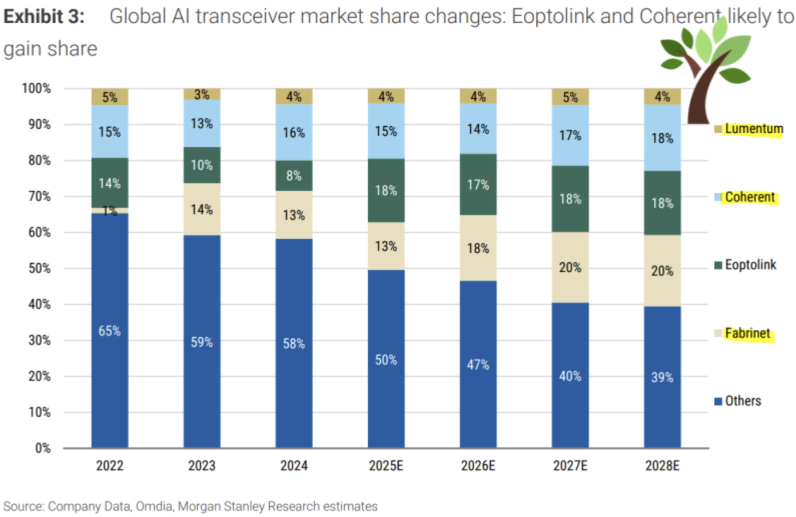
Major players:
- Fabrinet (NYSE: FN)
- Eoptolink (SHE: 300502)
- Coherent (NYSE: COHR)
- Lumentum (NASDAQ: LITE)
- Zhongji Innolight (SHE: 300308)
Optical-transceiver market growth: CY25 $18B → CY28 $50B
Per Morgan Stanley analysis, the AI optical-transceiver TAM is expected to grow from $18B in 2025 to $50B in 2028 — roughly 2.8×.
| Metric | 2025 | 2028 | Increase |
|---|---|---|---|
| AI optical-transceiver TAM | $18B | $50B | ~2.8× |
| AI transceiver units | 41M | 95M | ~2.3× |
| 800G + 1.6T transceiver share | 49% (~20M) | 84% (~80M) | — |
Growth drivers — three forces operate in parallel:
- Quantity growth from AI infrastructure expansion — as GPU counts within a single cluster grow, interconnect links scale at faster than 1:1.
- Quantity growth from copper → optical replacement — as systems push past 200G per lane, the copper domain shrinks and the optical domain expands. Optics likely to penetrate even into intra-rack interconnect.
- Price growth from the upgrade cycle to higher-spec products like 800G / 1.6T — mix shifts rapidly to higher-priced products.
(5) Implications
- Transceivers are the largest-revenue layer today and are simultaneously one of the most attractive, with both unit volume and ASP growing together.
- CPO adoption isn't replacing transceivers — it's closer to net-new demand added in the scale-up domain — and in scale-out, demand for pluggables / NPO transceivers is likely to remain dominant.
- New architectures like OCS act to further raise transceiver demand.
- The capacity bottleneck at the wafer (InP) → laser (especially EML) stage is likely to be the most direct supply-side constraint over the next several years.