2026 June Wk2 Datacenter Bottleneck(s) Brief

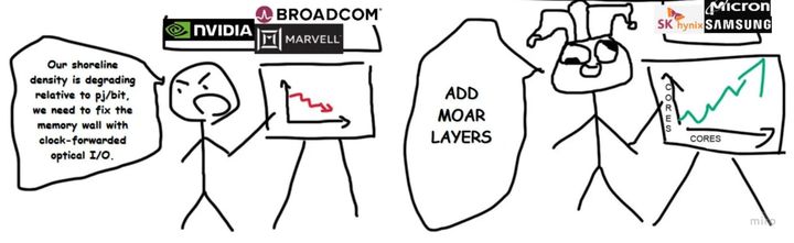
A Cruel Bottleneck's Thesis
- On the surface, it was a noisy week.
- A SemiAnalysis report on a SOCAMM2 spec downgrade, the scale-up CPO "delay" story, gas-turbine lead-time slips — read off the headlines alone, it is an easy stretch to lose the plot.
- The purpose of this note is to take each headline down to the fundamentals and verify it against earnings calls, channel checks, and disclosures.
- The conclusion first: most of this week's noise is
- (a) a re-report of a timeline that was already known,
- (b) an adjustment in form (packaging, module configuration, generation mix) rather than a break in direction, and (c) if anything, demand-side fundamentals were revised up on every earnings call.
1. Memory & Storage — The Conditions for a Cyclical → Secular Re-rating
1.1 Background
- Before going into the details, for the specific design of Nvidia’s Rubin GPU and Vera CPU, refer to each part of Vera Rubin Decoded.
- For the memory configuration of the Vera Rubin Compute Tray, refer to the section “Compute Was Never the Bottleneck — Moving Bits Is.”
SemiAnalysis
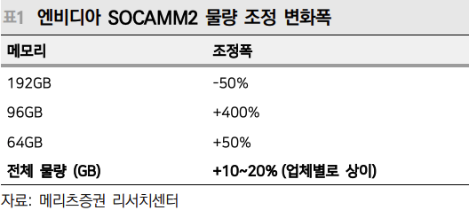
- In an institutional research note, SemiAnalysis estimates that the SOCAMM capacity loaded into a VR200 NVL72 rack will drop by 49%.
- For the VR200 NVL72 rack, they had expected the DDR5 (SOCAMM) rack capacity — excluding HBM — to be 55TB; due to allocation limits, the new estimate is 28TB.
- The SOCAMM2 destined for the Vera CPU was originally cited at 1.5TB (192GB × 8 stacks per module); it will now be 768GB (96GB × 8 stacks per module).
- Per-rack price moves from $7.6M (at 55TB) to $6.8M (at 28TB). Since that is a $0.8M reduction in SOCAMM cost alone, the rest of the BOM ex-SOCAMM works out to $5.97M, and
- SOCAMM's share of the BOM falls from 21.4% (at 55TB) to 12.2% (at 28TB).
- The VR200 NVL72 rack price itself is down only 10.5% ($7.6M → $6.8M), so from the customer's standpoint it makes little difference.
- The total LPDDR5x bit demand Nvidia procures is unchanged — only the per-rack capacity spec for the VR200 NVL72 was changed.
- The read-through: demand is very high while DRAM supply is tight. The most likely explanation for this spec change is not some other factor but precisely a "demand is high but volume is short" condition.
- For Nvidia, selling "more chips" is good for both revenue and margin.
- the Vera CPU used in the VR200 NVL72 head node,
- the Vera CPU Standalone rack used for orchestration,
- the CPU paired with the BlueField DPU, and so on,
- With Vera CPU demand confirmed high but no additional LPDDR5x available, that is exactly why this decision was made.
- Across the value chain, you can expect the unit volume (Q) of rack-scale products to hold or grow.
BNP Paribas Analyst Comment
- Sees DRAM and NAND ASP peaking in mid-2026 and rolling over — pulling the peak forward by a year from the previously expected mid-2027.
- Three reasons: (a) global smartphone shipments down 14%, (b) CXMT/YMTC capacity expansion, (c) memory consumption in other industries falling because of the price spike.
Rebuttal to (a)
- LPDDR5 demand is already being offset by expanded adoption of mobile-grade low-power LPDDR5 in AI servers (SOCAMM, etc.), so it is not a problem, and
- Apple too is willing to sacrifice GPM to grab a big share gain in the high-end smartphone market while the window is open.
Rebuttal to (b)
- CXMT/YMTC are not getting the equipment they want and are bottlenecked; the MATCH Acts have been introduced to tighten that bottleneck further in 2H.
- HBM3 is also delayed, and the situation is tight enough that the CCP itself has twice this year asked for production expansion.
- On DRAM wafer starts alone they look formidable, but CXMT's yield is reportedly below 50% (again because of the equipment-import problem), so real output (bit output per wafer) is about half that of SEC/SKH/MU.
- Overcoming this requires the domestic Chinese equipment ecosystem (Naura, AMEC, Piotech, SMEE) to mature further than it has — and that still needs time.
Rebuttal to (c)
- The market is being driven by the bit demand of hyperscalers that can absorb today's memory prices, so it will be offset by AI servers taking a rising share of total DRAM and NAND demand.
1.2 Weekly Industry Updates
JPM (6/2):
- Sees rapid growth in PCIe 6 and LPDDR5X demand driven by the Vera CPU.
- The new AI-PC product N1X carries 128GB of LPDDR5X — an order-of-magnitude jump from the typical 12–16GB in existing PCs.
SK Hynix (KRX: 000660):
- Announced doubling DRAM WSPM (Wafers per Month) over the next five years.
- ~530k/month at end-CY25 → ~745k at end-CY28 → ~865k at end-CY29 → 1M+ once the first Yongin cluster phase is completed at end-CY30.
- That is a 15% five-year CAGR — hard to read as an oversupply signal. The swing factor is the ability to secure 50+ EUV tools across CY28–30.
Kioxia (TYO: 285A) Investor Day:
- Raised its long-term CY28 NAND TAM to 1,807EB (3-year CAGR 22%),
- and sees the shortage persisting at least through 2027.
- eSSD market: CY25 295EB → CY28 900EB+,
- with AI-inference memory/storage demand growing 86% per year as the driver.
TD Cowen:
- HDD makers may keep raising prices aggressively into CY27,
- with CY27 HDD ASP reaching ~$20/TB (+20% YoY).
- On that basis Seagate (NASDAQ: STX) CY27 EPS $45–50 (consensus low-$30s), Western Digital (NASDAQ: WDC) ~$30 (consensus low-$20s) — roughly 40% upside.
- The key is not demand but that pricing power is becoming consensus.
1.3 SanDisk's LTA — Not a Volume Contract but a Margin-Defense + Financing Contract
SanDisk's (NASDAQ: SNDK) LTA minimum GPM is around 80% — far above the DRAM-industry LTA floor (~60%). Roughly 30% of CY27 capacity is already locked under LTAs, with a long-term target of 80%. It is the most aggressive LTA structure in NAND.
SNDK's formal name for it is the NBM (New Business Model).
- As of the FY Q3'26 earnings call (4/30), 5 signed (3 in Q3 + 2 in Q4), with more in negotiation.
- Structure: (a) up to 5-year terms, (b) quarterly committed volume that ramps over the contract life, (c) a fixed + variable price blend (SNDK takes the upside when prices rise; the customer takes part of the upside when they fall).
- The 3 Q3 signings alone put minimum contract revenue (RPO, at floor pricing) at ~$42B — in management's words, "providing visibility, pricing protection, and more consistent, durable returns."
Why the LTA is a "risk-distributing financing instrument" — on the $11B+ in financial guarantees:
- The key point is that these are not simple take-or-pay commitments but a structure where the customer posts collateral.
- The financial guarantees across the 5 deals total $11B+, in two forms:
- (a) prepayment: $400M already booked on the Q3 balance sheet,
- (b) financial instruments administered by third-party institutions (bank guarantees / letters of credit) that trigger immediately and pay cash to SNDK if the customer fails to take the committed volume.
- In management's words, "billions of dollars of collateral through various financial instruments that will survive for the life of these contracts."
Why "risk-distributing financing":
- For SNDK, which runs the fabs, whatever it produces it must sell;
- the NBM locks that demand in via contract and collateral.
- (1) The $400M prepayment is interest-free working capital / CapEx funding provided by the customer, and
- (2) the bank guarantee makes the customer (and the guaranteeing bank) absorb NAND demand risk — effectively financing fab utilization against customer contracts rather than SNDK's own credit.
- The risk shifts from "I (SNDK) carry the full burden of expansion and bear the cycle's demand risk" to "the customer posts collateral and underwrites the utilization of my (SNDK's) fabs."
Verifying the outcome:
- In the quarter, SNDK hit its net-cash target and announced a $6B buyback.
- It financially demonstrates that NAND is shifting from a cycle that consumes capital to a structure where customer collateral holds the cycle up.
- The 80% minimum GPM (margin defense) + $11B in collateral (financing) bundled inside a single contract is what differentiates SNDK's LTA.
In sum, the LTA's "$11B in financial guarantees / $42B RPO / over one-third of FY27 revenue secured" is the core mechanism enabling the cyclical → secular transition of §1.4 — the point being that this is not a "shake hands, sign, take a photo, done" commitment between seller (SNDK) and buyer, but a "bank-guaranteed backlog" that collateral genuinely backstops.
1.4 Why the LTA Can Become the Industry Standard — From the Buyer's Incentive
- When DRAM/NAND was 10–15% of datacenter CapEx, quarter-by-quarter price negotiation was rational; now that it is 40%+, the buyer too is better off locking in volume ahead on the assumption that "prices grind higher like HDD" — it helps datacenter ROI math and CapEx visibility.
- bit supply YoY +20–25% × ASP YoY +20–25% = structural profit growth of +44–56% YoY.
- This is not a bet on rising prices but on visibility of long-term profit growth; once secured, a higher P/E than today's can be justified on a cyclical → secular premise — the same logic structure as CPU names trading at CY27 P/E 30+ and optical names at 25–30x today.
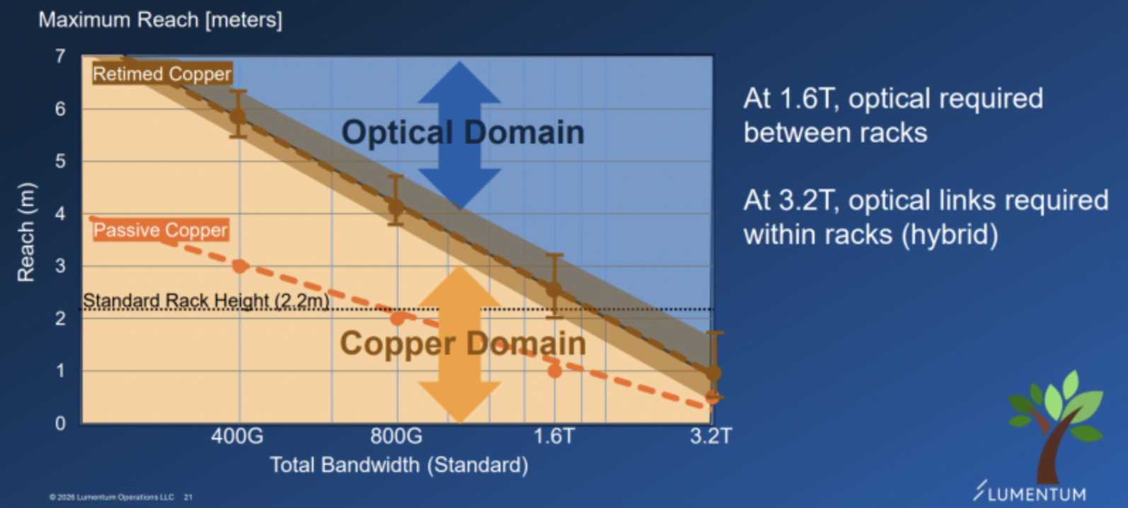
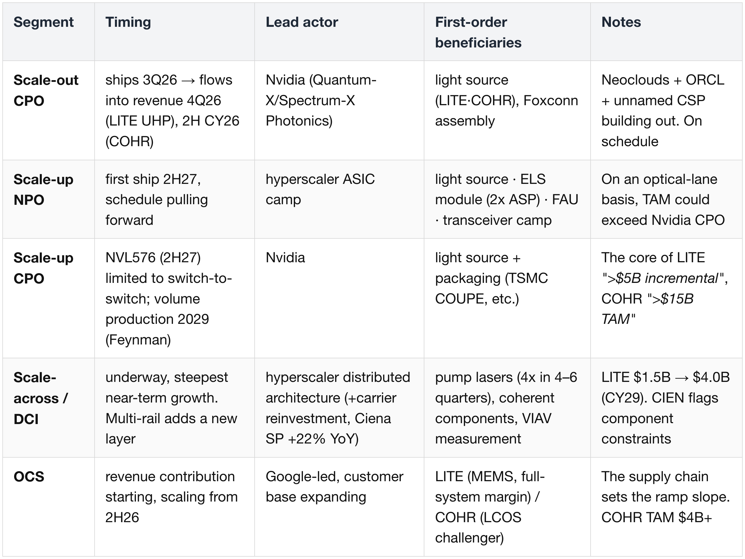
2. Optical Interconnects — CPO · NPO · OCS · Scale-across
2.1 Background
- For the detailed engineering transition in optical interconnects, from pluggables to CPO, refer to On CPO Pt.1.
SemiAnalysis commented on AI hardware broadly in an institutional note. On optics specifically:
- (a) CPO volume production after 2028-2029,
- (b) on a CPO-system basis, 19% yield (assuming 95% optical-engine attach yield and 32 COUPE per accelerator, system yield is 0.95^32 ≈ 19%).
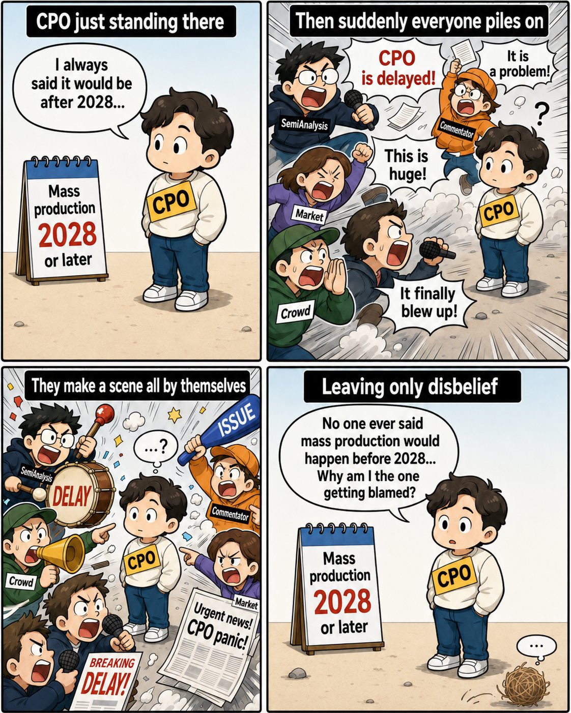
- Volume production / shipment of scale-up CPO switches was (effectively) already understood by investors to begin in 2029, but without the broader context many simply heard "CPO production is delayed" and dumped the stock.
- So what networking gets used during the CPO ramp-up window? The view: in the interim, many NPO projects ramp to meaningful volume.
2.2 The Frame — CPO and NPO Are One Continuum
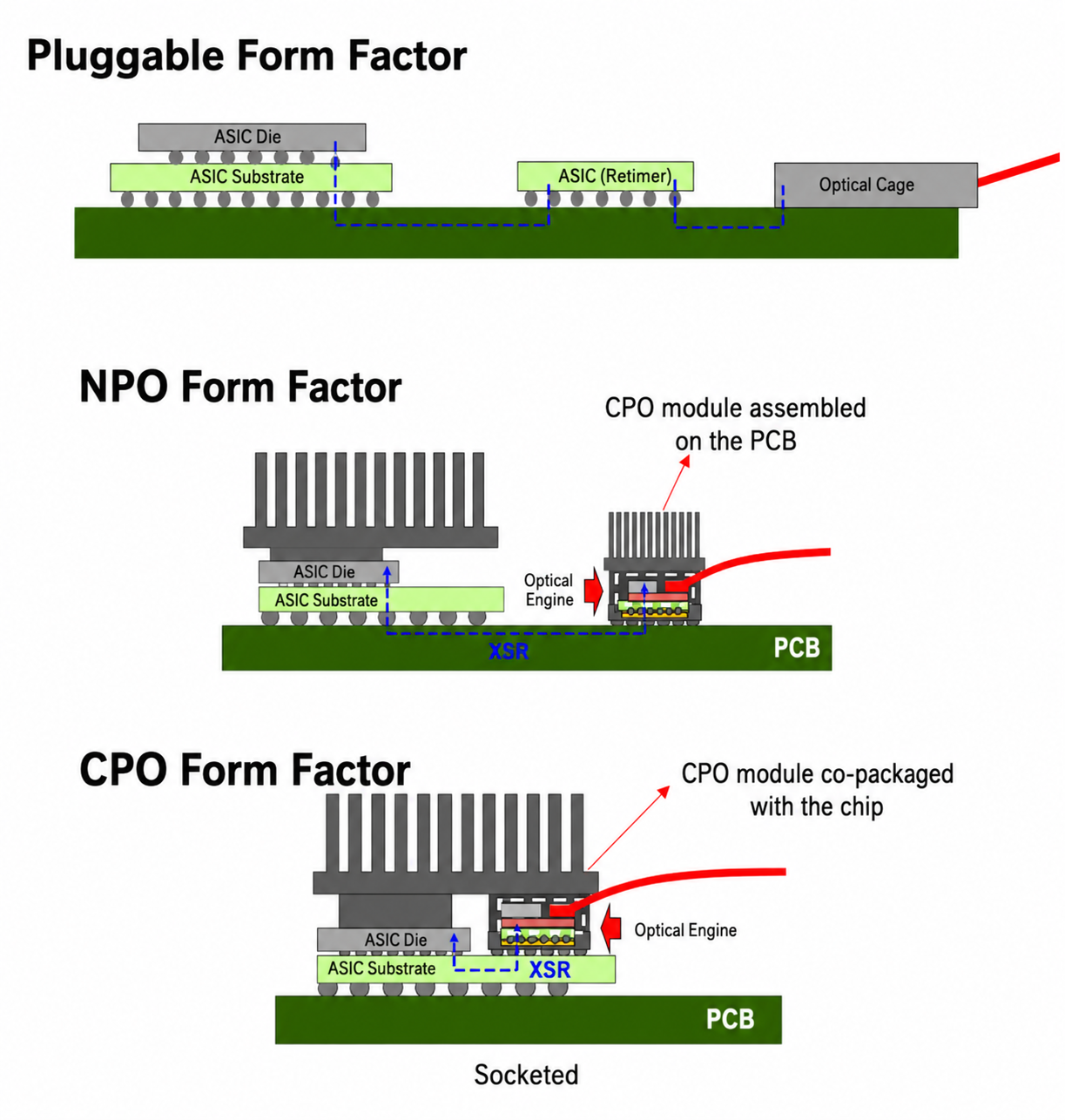
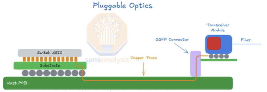
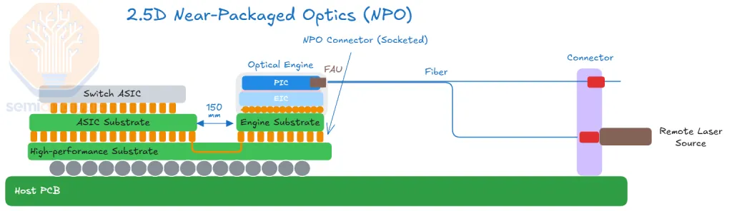
- Whether CPO or NPO, the requirements are the same: (a) Laser Source (UHP CW laser / ELS), (b) Fiber Array Unit, (c) PIC/EIC.
- The only difference is where the PIC/EIC is finally packaged (on the Switch ASIC substrate → CPO; off it → NPO). In practice it only changes which player does the packaging; the broad trend in demand for the light source (laser), FAU, and optical components is unaffected.
- So "scale-up CPO delay"-type headlines should be read not as a break in the scale-up optical-interconnect penetration thesis but as an adjustment in the specific packaging form and in each form's adoption timing. At the system level the architecture is consistently moving toward higher bandwidth density, lower power, and higher integration.
2.3 Scale-up — The Real Game Is Effectively From 2029; the Interim Belongs to NPO
Timeline (after institutional cross-checks — the key point being that nothing announced this week is new):
- Volume production / shipment of scale-up CPO switches begins in 2029 (the Feynman ramp). Investors already understood CY29 production.
- The CY 2H27 Rubin Ultra NVL576 scale-up CPO applies only to NVSwitch-to-NVSwitch (not direct to the GPU). The project scale is not large enough to move the needle.
- The Rubin Ultra rack architecture looks likely to stay on Oberon. The Kyber 800 VDC structure is not the mainstream adoption before Feynman (introduced post-2028); compute die per rack stays at 144 and power is revised down from the original ~1MW expectation to below 500kW.
- With 800VDC pushed out, there is also no near-term catalyst to justify the multiples of pure WBG power-semiconductor plays like WOLF or NVTS.
- With 800VDC pushed out, there is also no near-term catalyst to justify the multiples of pure WBG power-semiconductor plays like WOLF or NVTS.
- In the interim, a number of NPO projects ramp to meaningful volume — still a favorable setup for incumbent transceiver and optical-component makers.
NPO momentum (Lumentum (NASDAQ: LITE) comments, Mizuho Tech Conf. + Needham NDR):
- Nvidia leads on CPO while the hyperscaler ASIC camp is evaluating NPO. Over the past two months non-Nvidia customers' interest in NPO has visibly risen and adoption schedules are being pulled forward — first shipment of an NPO-version switch in 2H27.
- The ASIC camp is saying "to exceed Nvidia's performance you have to lay more 1.6T lanes into the rack backplane," so even though it looks small in rack count, on an optical-lane basis LITE judges the ASIC NPO opportunity to look larger than the Nvidia CPO opportunity.
- The moment the per-lane move to 200G hits copper's physical limit, optical-backplane adoption turns aggressive. Even going NPO, selling in ELS-module form carries 2x the ASP of a standalone light-source chip (UHP laser).
Earnings-call cross-check:
- LITE FY Q3'26 earnings call (5/5):
- "our largest single growth driver, scale-up CPO is still very much in its infancy" — it has already taken billions of dollars of orders centered on scale-out, scale-up will be far larger, and done right it is "somewhere greater than $5 billion of incremental revenue."
- Expects a "massive supply-demand imbalance" in CPO. The laser volume that must ship in 2027 — scale-out and scale-up demand overlapping — is "really a massive step-up."
- Coherent (NYSE: COHR) FY Q3'26 earnings call (5/6):
- scale-out CPO revenue starts ramping in 2H CY26; scale-up CPO revenue starts ramping in 2H CY27.
- Frames CPO as ">$15 billion of incremental addressable market" and reaffirms the March strategic partnership with Nvidia (multiple CPO product lines).
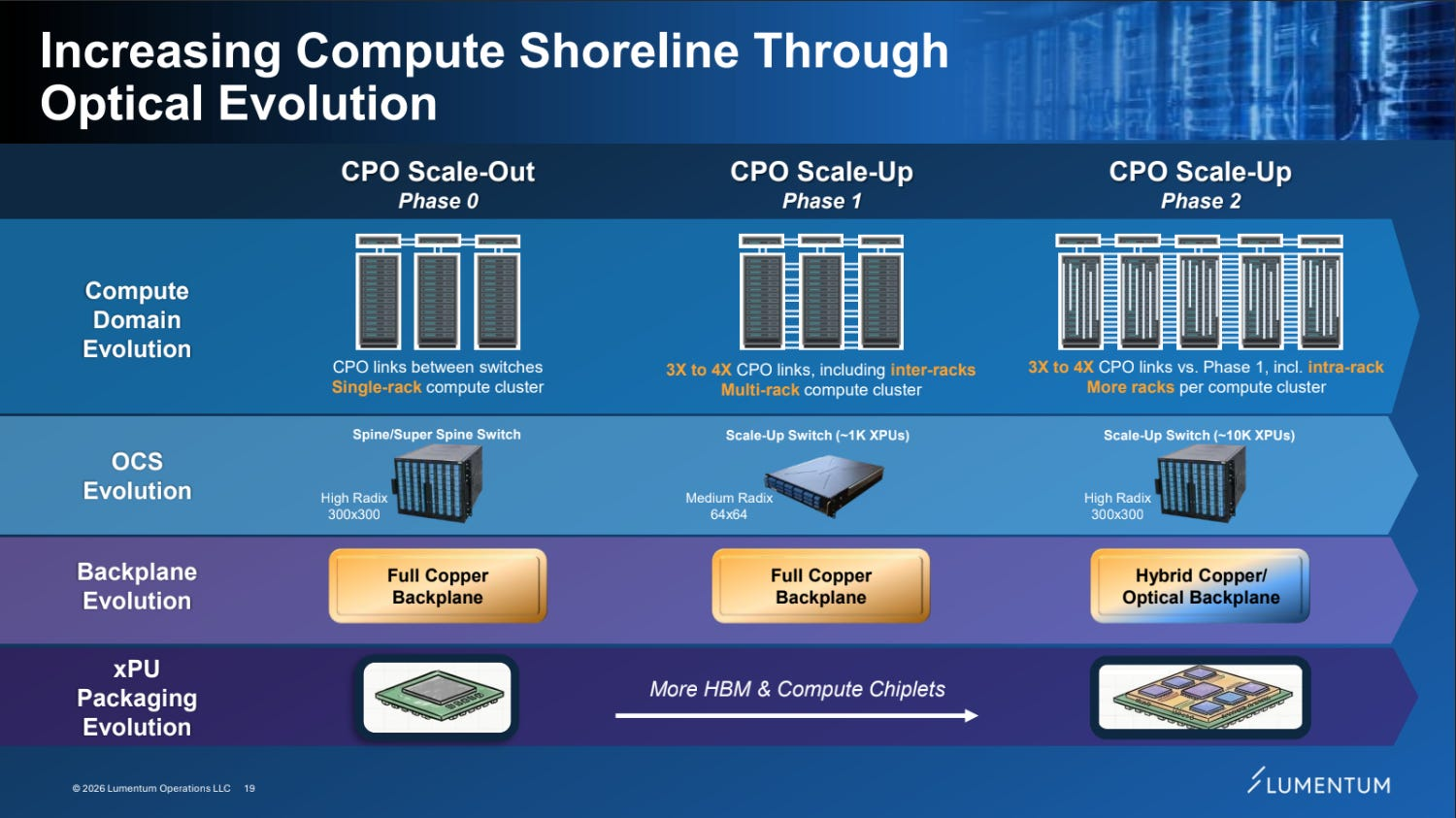
- On the CPO scale-out & up ramp curve:
- Phase 0 (SN6810, H2 CY26) — 25% of VR NVL72 deployments → Phase 1 (CY27) — switch mix 60%+ → Phase 2 (Feynman) — "all CPO,"
- CPO content per rack scales 9–16x across generations. Even with CPO/NPO coexisting, this is consistent with the long-run view that optics structurally takes a rising share inside and outside the cluster.
2.4 Scale-out — Proceeding on Schedule; Transceivers Benefit First
Scale-out CPO is proceeding on the original schedule. At Computex 2026 Jensen stated clearly that CPO will proceed as planned.
- Neoclouds (CoreWeave, Lambda), Oracle (NYSE: ORCL), and one unnamed major CSP are building out scale-out CPO, and
- Foxconn's (TPE: 2317) CPO mass production is on track (supply-chain feedback positive).
- LITE: the UHP-laser ramp for Nvidia scale-out CPO is on plan.
- Shipments start 3Q26, meaningful revenue from 4Q26 — reaffirmed on the FY Q3'26 earnings call as "on schedule to both deliver meaningful revenue in our December quarter and fulfill the multi-hundred million dollar purchase order slated for the first half of calendar year 2027." Collaboration with multiple CPO customers in pluggable turnkey ELS-module form is underway.
- COHR: initial scale-out CPO revenue starts 2H CY26 (same timeline as above).
- The key point, independent of CPO vs NPO, is that light-source demand is the same — it is only a question of which packaging it ships in.
In the interim, cash flow is still led by transceivers:
- LITE FY Q3'26:
- revenue $808M (record YoY),
- cloud modules +40% QoQ,
- 1.6T transceivers ramp from FY Q4'26 (some carrying its own CW laser).
- laser-chip shipments 2x the year-ago quarter,
- EML shipment-growth target of +50% YoY through the December 2026 quarter.
- EML takes most of the 1.6T adoption volume (consistent with Mizuho's comments).
- The constraint is supply, not demand.
- Applied Optoelectronics (NASDAQ: AAOI) FY Q1'26:
- completed first 800G volume shipments + won a first 1.6T volume order from another long-standing hyperscaler customer.
- 800G/1.6T capacity 100k/month → 650k by end-2026 → 930k by end-2027 target,
- with a mid-2027 datacenter-transceiver revenue target of $471M/month.
- But the CPO-grade ELSFP has not even begun hyperscaler qualification — the structure where AAOI actually benefits as pluggable life extends is consistent with the call (the entire call was a transceiver-capacity story, with no mention of CPO revenue).
- Note (10-K vs call tone gap): in LITE's FY2025 10-K (filed 25-08-19), co-packaged optics gets a single-line "advanced packaging schemes" mention. That it became the call's central topic within a year is itself evidence of CPO's commercialization pace.
2.5 Scale-across — The Steepest Near-term Growth; Multi-rail Adds a New Layer to the Industry
- Hitting the power and space limits of a single building, hyperscalers are shifting to structures that link geographically dispersed compute domains.
- LITE FY Q3'26 earnings call: "As hyperscalers exhaust the power and space limits of individual data center buildings, they are shifting to distributed architectures... These scale-across networks require high-bandwidth synchronization across multiple data centers."
- Explicitly names the scale-across product line as one axis of margin expansion.
- On Ciena's (NYSE: CIEN) Q1'26 results, the key supply-constrained components were modems/DSPs and pump lasers — evidence that scale-across demand is already tight at the component level.
- What multi-rail means:
- Where prior optical upgrades made "one lane faster" (per-lane 400G → 800G, faster wavelengths, higher-speed modules),
- multi-rail increases the number of optical paths usable simultaneously.
- It grows not speed but the network's physical density and parallel connection count — as paths multiply, amplification spans, coherent links, and fiber all grow with them, so it adds a new optical-demand layer on top of the existing optical network.
- The pump-laser demand mechanism:
- An optical signal weakens over distance, and the scale-across legs — datacenter ↔ datacenter, campus ↔ campus, city ↔ city — require intermediate amplification.
- Since the pump laser is the core component of the amplifier, more optical paths → more amplification demand → directly more pump-laser demand.
- LITE's pump-laser shipments are seen growing 4x over the next 4–6 quarters (Needham NDR),
- with the current ~$1.5B business growing into a $4.0B market by CY29.
- Production is at the Takao fab (Japan) + Caswell fab (UK).
- COHR FY Q3'26: Communications-segment revenue +16% QoQ / +60% YoY — driven by DCI, scale-across, and traditional telecom, with a strong growth guide for the current quarter as well.
- Carrier demand is recovering too — at Ciena, service-provider (carrier) revenue grew ~22% YoY this quarter (FY Q1'26, mostly MOFN-driven), and full-year FY26 revenue-growth guidance was raised from 24% → 28% (midpoint). Carriers, having underinvested in optical infrastructure for the past five years, are starting to reinvest:
- hyperscalers are the main driver today, but
- when carriers begin reinvesting in optical infrastructure (metro, long-haul DCI, coherent transport), Viavi (NASDAQ: VIAV) has large exposure.
- It maps straight to operating leverage because the beneficiary segment — NSE (Network and Service Enablement) — is almost entirely volume-driven.
- The incremental-revenue-to-operating-income conversion is ~40–45% ("for every incremental dollar in NSE... about $0.45 dropping to bottom line" — Oleg Khaykin, CEO), so recovering revenue falls straight to operating income.
Multi-rail scale-across beneficiaries: LITE — selling DCI-bound product lines (pump lasers, Narrow Spectral Linewidth Lasers, etc.) at high margin. The most direct exposure.
VIAV — the beneficiary segment is NSE (Network and Service Enablement), specifically
- (a) lab/production instruments (gear with which optical modules, high-performance semis, and NEMs (Network Equipment Manufacturers) validate each component during R&D and volume production),
- (b) field instruments (on-site install, activation, assurance),
- (c) high-speed Ethernet test added via the Spirent acquisition (800G → 1.6T → 3.2T integration).
- The OSP (Optical Security and Performance) segment (3D sensing, anti-counterfeiting) is unrelated to datacenter optics.
- On the FY Q3'26 earnings call, NSE revenue +54% YoY ($321.5M) was said to be driven by the "data center ecosystem... in support of AI data center build-out,"
- with scale-across demand named directly: "strong demand across all data center segments. Scale up, scale out and scale across."
- VIAV sells instruments that characterize, validate, and assure optical signals and links, so "measurements needed" = the total count of points and instances where an optical signal must be measured. Rising measurements needed therefore shows up in revenue along two branches:
- (1) More DCI = more "places to measure": each new DCI/coherent link becomes a measurement target at every stage — R&D validation (lab) → volume test (production, individual per-module/component test before shipment) → field commissioning and operational assurance (field).
- (2) Multi-rail = greater "measurements needed": rather than raising one path's speed, it increases the number of parallel optical paths, so the test burden scales with the number of parallel rails, not per-lane speed.
- On top of that, each network-speed step (800G → 1.6T → 3.2T) needs new test capability (the Spirent integration covers up to 3.2T).
- Multi-rail/DCI lands on VIAV not as "one faster line" but as "more things to validate" (number of measurement points × speed grade).
AAOI
- AAOI does not sell DCI-only components like coherent/ZR transceivers or pump lasers. Per the Q1'26 earnings call,
- datacenter revenue is intra-datacenter PAM4 transceivers (100G 41% / 200G+400G 46.7% / 800G 5.6%),
- with the rest CATV RF amplifiers and telecom.
- So its scale-across benefit is indirect, via two paths:
- (a) what multi-rail / distributed architectures ultimately increase is total optical-lane count, and traffic heading to campus/DCI gateways is still aggregated through standard intra-datacenter PAM4 lanes (800G/1.6T), so rising lane count flows down into transceiver demand.
- (b) to the extent scale-across / multi-rail extends the pluggable ecosystem's life, the transceiver-capacity story before the CPO transition (650k → 930k per month) stays valid longer.
- AAOI is best classified not as a DCI-component beneficiary but as a beneficiary of "more total optical lanes + longer pluggable life."
2.6 OCS — A Separate Industry Axis, but the Same Context
For how OCS works, as well as the two technology roadmaps of LITE + Google versus Coherent, refer to On CPO Pt.5.
LITE
- The recently announced multi-year, multibillion-dollar purchase agreement secures long-term growth. But the ability to expand output is constrained by the supply chain ("considerable tightness... due largely to the significant step-up in requested output").
- The company itself names OCS as "the biggest single tight rope" among its three ramps (pump lasers, CPO, OCS). Up to $1B ARR it builds internally; above that it uses contract manufacturing while redirecting internal capacity to common-component production — pursuing economies of scale and margin uplift at once.
- In the earnings-call Q&A, alongside mention of a Google TPU v8 inference rack (1,152 TPUs) and a 130k-TPU training rack, it discussed 300/500-radix OCS demand — with the tone that v8's OCS pull is not much different from v7. In a scenario where TPU volumes are revised up, OCS is the most direct derivative beneficiary.
COHR
- Raised the OCS market opportunity to $4B+ (use cases expanding across DCI, scale-out, scale-up). It has resolved the production bottleneck and is producing and shipping in volume from two fabs.
The MEMS vs LCOS debate continues:
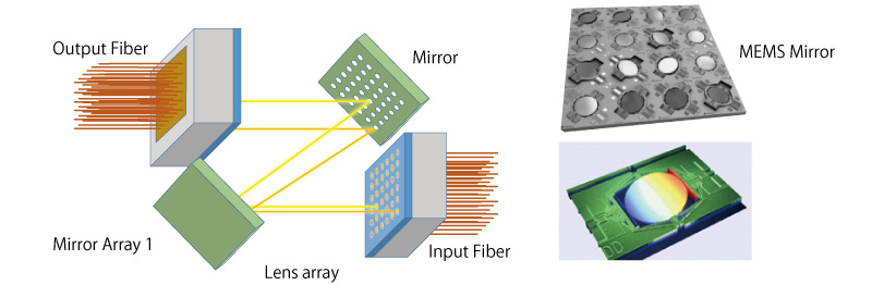
- LITE backs MEMS (Micro-Electromechanical Systems; developed primarily by Google; 20+ years proven in carrier long-haul networks, structurally low optical loss — and hyperscalers are most sensitive to loss). LITE expects hyperscalers to stick with MEMS.
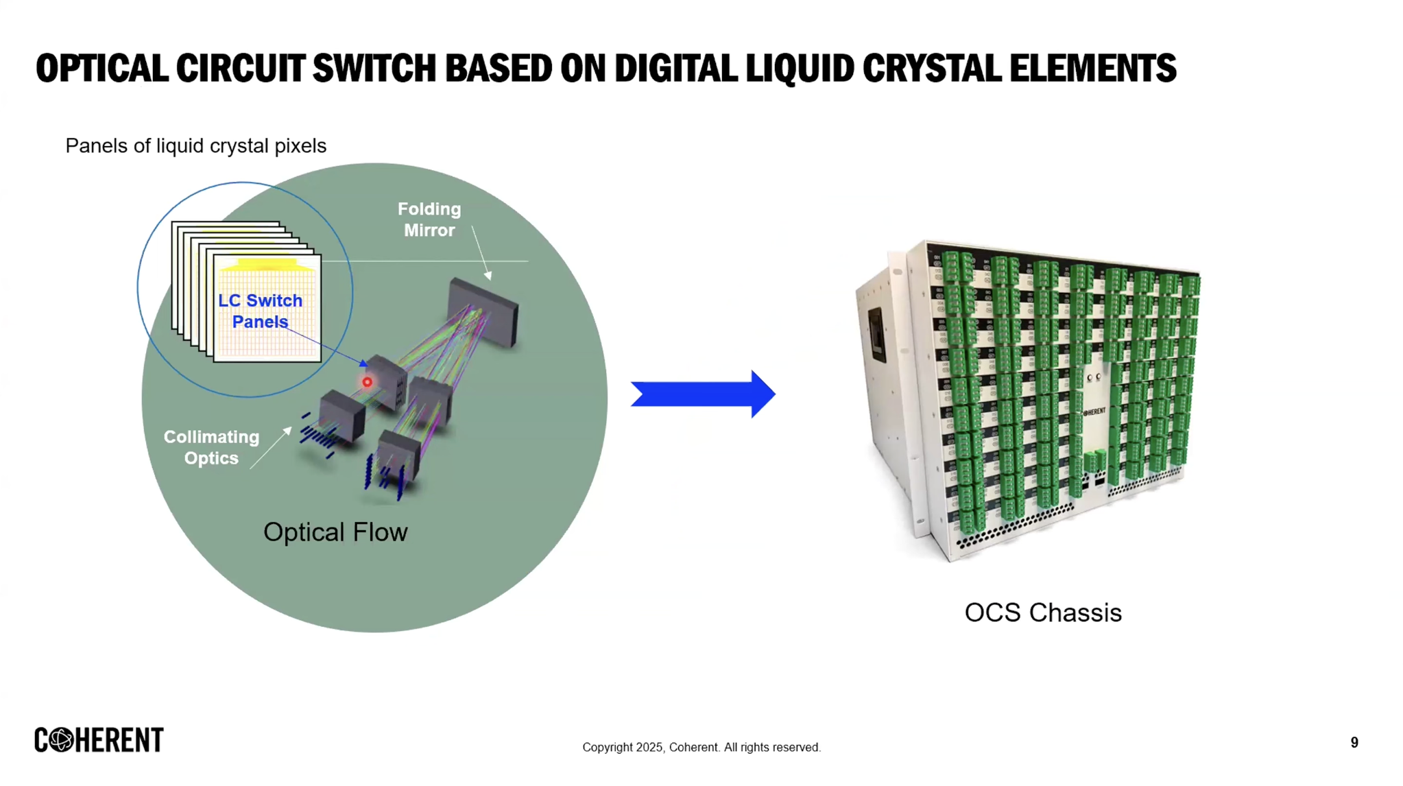
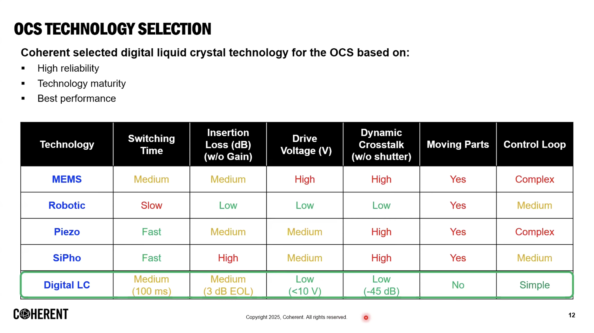
- COHR backs LCOS (Liquid Crystal on Silicon Optical Circuit Switch; because MEMS physically moves mirrors it has a long-term-reliability weakness; COHR argues that even at 2–3x the cost, LCOS can penetrate the future hyperscaler OCS market on long-term reliability; COHR is the primary supplier).
2.7 The Common Bottleneck — InP Wafer Capacity, and This Week's Geopolitical Variable
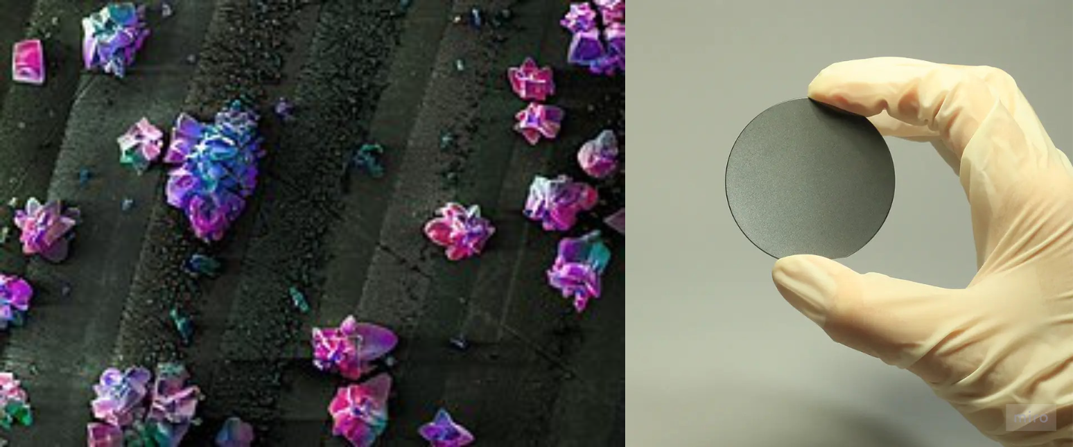
Whichever networking is chosen, a light source is needed, and the light source is bound to InP capacity. For both companies, large-diameter wafer processing is the simultaneous lever for margin and volume.
LITE
- Converting the Sagamihara fab from 3-inch → 4-inch InP (1.8–2x effective dies per wafer).
- 1.5 fabs at full utilization, with room for additional capacity in CY27.
- Plans +50% capacity from December 2025 to December 2026.
- Acquired a fifth InP fab (Greensboro, North Carolina) in March — but it runs from 2028, so it is not in current guidance numbers.
- Where the past year's margin expansion was price-led, the next leg is cost-reduction-led (large-diameter wafer processing — depreciation and energy do not scale with wafer area).
- 6-inch InP wafers are on hold due to volume-yield difficulty; the strategy is to absorb quickly once others succeed.
COHR
- 6-inch InP wafer mass production is the key differentiation point — COHR itself calls it "a key driver of our long-term capacity expansion and a meaningful differentiator."
- Why? InP (indium phosphide) is the substrate for active optical components like EML, CW laser, and photodiode, and dies per wafer scale with area (the square of the diameter).
- On COHR's numbers, a 6-inch wafer can produce 4x the dies of a 3-inch at less than half the cost ("6-inch versus 3-inch is more than 4x as many devices at less than half the cost").
- Tool depreciation, energy consumption, and process steps are fixed costs per wafer, so spreading them over more area drives unit cost down and GPM up (same principle as LITE's 3→4-inch conversion, but COHR is a generation ahead).
- The real moat is yield:
- InP is a more brittle compound semiconductor than silicon, so the larger the diameter the greater the cracking and yield loss — which is why most of the industry stays at 3-/4-inch.
- COHR says its 6-inch yield "already exceeds" its own 3-inch line across all three components (EML, CW laser, photodiode) — solving the hardest problem (large-diameter InP yield) first is the core differentiation.
- As seen in the LITE block above — where LITE holds off on 6-inch and plans to absorb the know-how after others succeed — COHR's 6-inch lead is a real gap.
- Progress + whether it shows in the financials:
- First shipment of transceivers carrying 6-inch components begins contributing to both revenue and GPM.
- Internal InP capacity targeted to double by year-end and double again by end-CY27.
- Q3 non-GAAP GM 39.6% (+57bp QoQ / +105bp YoY), OIM 20.3% — among the three GPM-expansion drivers (cost reduction, yield improvement, price optimization), 6-inch InP is starting to push both cost and yield up at once. Investor-Day target GPM >42%.
- Supply-chain site diversification:
- Sherman (Texas) — what COHR calls "the world's most advanced indium phosphide production site" —
- is the center of the CPO CW-laser ramp (including Nvidia-partnership volume).
- Zurich is the third 6-inch site — geographic diversification of capacity and a hedge against the China InP-export risk discussed below (COHR currently receives InP from China; AXT is one of its suppliers).
- Other sites include Fremont (CA) and Järfälla (Sweden).
- The connection to CPO (why 6-inch is strategic):
- The CPO content covered by the Nvidia partnership ($2B equity + 10-year supply agreement) is broad — high-power CW laser plus ELS module, FAU (micro-lens array, PM fiber), isolator, and TEC — and the starting point for that light source is the InP substrate.
- With InP a common industry bottleneck, whoever volume-produces cheaper and more InP dies first captures share in CPO mass production (scale-out 2H26 → scale-up 2H27), so 6-inch capacity = the ability to convert CPO upside into actual volume.
- On the demand side both companies say "supply runs far below demand" — the industry-wide InP constraint is named on COHR's earnings call as "industry-wide constraints in indium phosphide." COHR's backlog runs to CY2028, and LTAs extend to end of the decade.
Additional comments
- While ramping its own 6-inch InP wafer production, COHR simultaneously sources laser modules from an external supplier to meet customer demand. That supplier is LITE. (At the Morgan Stanley TMT Conference 2026, COHR CEO Jim Anderson referred to LITE as both a "good partner" and a "supplier.")
- Of course, as 6-inch InP wafer output scales to target, EML procurement from LITE is expected to decline or slow around H2 '27.
This week's added geopolitical variable — China pressuring/delaying InP export approvals
- InP is the base material for optical chips. Exposure varies widely by company:
- AXT (NASDAQ: AXTI) — the most directly hit. Headquartered in the US, but its InP crystal growth and wafer production are in China, so export approval for Chinese volume is the company's biggest issue. Both LITE and COHR source InP from AXT.
- COHR — currently receiving Chinese InP volume, and raised this issue directly on a recent China visit. Some exposure exists.
- LITE — sources InP substrate/wafers from Japanese suppliers (Sumitomo Electric (TYO: 5802), JX Advanced Metals (TYO: 5016)), so it can diversify supply-chain risk.
- Read-through: with InP capacity the common bottleneck, the region of substrate sourcing becomes a new axis of differentiation. Whoever has vertical integration (in-house crystal growth) or a Japanese sourcing line holds the relative edge (that is LITE).
2.8 Networking by Segment
In sum:
- scale-out is on schedule; scale-up in CPO form is pushed to 2029, but
- that gap is filled by NPO + optical transceivers + OCS + scale-across,
- so for companies holding light-source and InP capacity, total demand holds or grows under any scenario.
- The packaging-form debates (CPO vs NPO, MEMS vs LCOS) are a question of how parts are allocated within the value chain, not a question of the direction toward optics.
3. Datacenter & Power — Redefining the Bottleneck
3.1 The Bottleneck Is Not the Turbine Factory but the System
Permitting, gas-turbine and transformer lead times, and skilled-labor shortages are the usual delay factors cited — but permitting was always a structural issue, and the two newly important ones (turbine lead times, skilled-labor shortages) actually fold into one cause:
- GE Vernova (NYSE: GEV) CEO @ Bernstein conference (260527): demand being high does not let you pull capacity forward. Even if you build the turbine, if the customer's site has no pedestal (installation base) ready, capital efficiency drops — the bottleneck is less the turbine factory than a system bottleneck spanning EPC, labor, on-site construction, permitting, and grid interconnection.
- Gas turbines and reciprocating engines do not produce power just by dropping the equipment on site. The on-site balance-of-plant is large, with a lot of EPC labor and process to get through — so turbine lead-time slips and skilled-labor shortages bundle into a single on-site bottleneck.
- Gas-turbine backlog has passed 100GW+, with large units booked past 2030 and mid/small units full through 2028 — because of bridge-power demand (temporary, interim generation pulled forward 1–2 years before grid connection).
3.2 Power-supply Channel Check (TD Cowen TMT Conference + Bernstein), the Widening of BTM Demand
- Lead times: among 800 VDC-related components, UPS and medium-voltage switchgear are slightly delayed.
- Cost: skilled-labor cost +30% YoY, reaching 40–45% of total construction cost on some projects. Construction cost runs $13–19M/MW by region (vs ~$12M in 2H25). The most-shortage trades are electricians, HVAC technicians, and subcontractors.
- NIMBY: now cited as nearly as much of a bottleneck as power procurement — the first time community acceptance has been this much of a bottleneck. The main drivers are noise and harmful-gas emissions from BTM generation.
- Bernstein comments:
- datacenter project pipeline +10% MoM (+29GW) over the past month → 324GW.
- capacity under construction 63GW as of May (+4.4GW).
- capacity slowed by NIMBY 34GW (+1.9GW), or 11% of the pipeline (up from 7–9% in Jul–Sep 2025, but stabilizing recently).
- The quality of BTM demand: geographic diffusion (Europe gradually strengthening, Asia rising at GW scale — India the steepest) + customer conversations shifting from short-term capacity leases to 5-year+ long-term plans — it is being recognized as structural, not temporary, demand.
- The grid: interconnection queues are saturated — utilities are screening projects on deposits, letters of credit, and take-or-pay terms. BTM / on-site generation is becoming a hard requirement.
3.3 The Shift in BTM Generation Mix — Gas Turbine → Reciprocating Engine · SOFC · BESS
- Rising gas-turbine prices create a preference for reciprocating engines, but reciprocating engines too — bottlenecked by rising on-site skilled-labor cost and NIMBY — end up at a similar $3,000–4,000/kW.
- SOFC is
- (a) entering a window of getting cheaper on an LCOE basis,
- (b) meeting lead times well and thereby improving project visibility, and
- (c) being pitched as a source that wins community acceptance — in a NIMBY-bottlenecked phase, the value of (c) rises. Unlike gas turbines / reciprocating engines, it emits no NOx/SOx and relatively little CO2.
- As gas-turbine projects get delayed by lead-time and on-site-install bottlenecks, the flow of outright cancellation and substitution to SOFC can strengthen. Representative cases from the past two months:
- (a) Oracle Project Jupiter 2.45GW,
- (b) Nebius DataOne 328MW.
3.4 Bloom Energy's Edge — Supply-chain and Delivery-scaling Capability Is the Moat
- For a detailed analysis of Bloom Energy’s strengths, along with its financials and valuation, refer to Datacenter Power Supply Pt.2.
It is not simply that they make SOFC, but that the capability to manage the supply chain and scale delivery to meet rising demand is itself the moat.
- SOFC is prefabricated, then trucked and installed to minimize on-site labor, so it is less affected by the labor bottleneck than gas turbines — a structural advantage in a phase where EPC is the system bottleneck.
Bloom Energy has shown such strength in component and supply-chain management that it weathered even the COVID supply-chain chaos without major disruption
- Bloom Energy's (NYSE: BE) 2020 earnings calls show:
- 1Q '20 (May): amid the early-pandemic chaos, it deployed new workflows to factories and install sites and kept the core business running while repurposing manufacturing resources to (1) refurbish 1,200+ ventilators, (2) stand up two hospital microgrids on an emergency basis, and (3) win FDA approval for a 4-person oxygen distributor — an episode demonstrating supply-chain and manufacturing flexibility.
- 2Q '20 (Aug): installed 306 systems in the thick of lockdown — +20% vs 1Q, which the company itself called "significantly better than we anticipated heading into April... a truly remarkable achievement." Quarterly installs rose despite COVID delays in the install process.
- 3Q '20 (Nov): achieved product cost −19% YoY through manufacturing-process and supply-chain improvements. "Our supply chain is fairly sophisticated in working with our vendors to improve their manufacturing processes, as well as simplify our product through engineering" — sustaining a system that generates 10–15% annual cost-down via supplier collaboration and design simplification, even through a crisis.
- Summary: a track record of raising installs, cutting cost, and even pivoting to emergency manufacturing through a global supply-chain crisis substantiates the assessment that "the CEO has deep command of component sourcing and manufacturing supply chains."
Crusoe-Tallgrass (Wyoming Cheyenne) update:
- Despite Crusoe's exit, the SOFC shipment plan holds — no order changes from other hyperscaler customers.
- Per additional reports, the lead customer was originally going to be Oracle but recently became Google — if it closes, a case of "supplying SOFC to a Google-backed neocloud."
- With a target start in early 2028, the 900MW SOFC delivery timing is around 3Q27.
- Of Tallgrass's 2.7GW on-site generation mix, SOFC is one-third (900MW) — the rest is 2x MHI M501JAC CCGT (1,328MW), 3x GEV LM6000 (153MW), 13x LM2500 (448.5MW) + 24x temporary LM2500 (828MW buffer; a design with large redundancy so power is not interrupted even when one 664MW-class CCGT is under maintenance).
Infrastructure-side confirmation from ORCL's 4Q26 results:
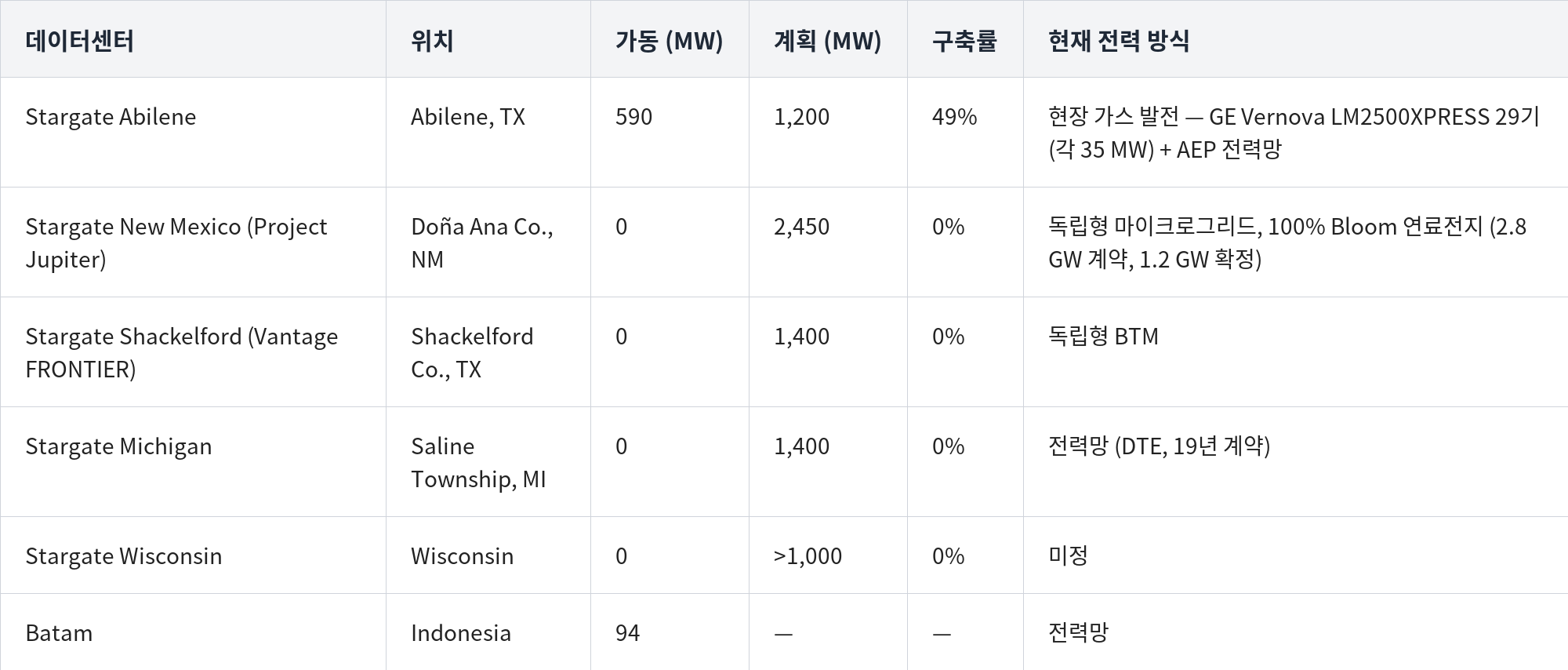
- Brought 1GW online in this quarter alone (a clear acceleration vs 1.2GW for all of FY26).
- (1) Stargate Abilene / Abilene (TX): 42% of campus capacity online + 35% more within 90 days + the remaining 23% online within the year.
- (2) Stargate Shackelford / Shackelford (TX): 115MW pre-energized + full online targeted by 1H27.
- (3) Stargate New Mexico / Doña Ana (NM): targeting 1H27 online on 2.45GW of Bloom SOFC.
- (4) Stargate Michigan / Saline (MI) by 2H27 and (5) Stargate Wisconsin / Port Washington (WI) targeting online by 2H27. Specific BTM power-supply means were not disclosed.
- The fundamental tone also improves each quarter: 3Q25 "demand is high" → 4Q25 "we can sell even if it's not OpenAI (as the client)" → 1Q26 "$50B financing taking shape + expanding BYOH / prepaid contracts."
4. Apple AFM 3 — MoE Inference Using NAND as Main Storage

4.1 AFM 3 Structure Summary (WWDC26 · 3rd-generation Foundation Model system card)
Apple licenses Gemini from Google (NASDAQ: GOOGL) under a ~$1B/year contract while splitting intelligence across three models:
- (a) AFM Cloud — Apple's own model (distilled from Gemini),
- (b) AFM Local — entirely Apple-developed,
- (c) AFM Cloud Pro — Gemini-based serving, but with the pretraining → post-training → RL stack implemented in-house.
Hardware mapping:
- Pretraining at scale on GCP TPU (favorable for large matrix multiplication + the large Pod-scale scale-up memory domain),
- serving optimized per model:
- AFM Core, Core Advanced, Cloud, Cloud (Image) on Apple Silicon,
- the largest model, AFM 3 Cloud Pro, on Nvidia GPU.
In model training, ASICs like GCP TPU / AWS Trainium may not overwhelm Nvidia GPUs on overall raw performance, but they can cut TCO (perf/$ + perf/watt) in specific segments.
- Large-scale pretraining of a hyperscaler's own models▸ Pretraining is the stage of training a model from scratch on massive data. Most of the compute is large-scale matrix multiplication (GEMM), and the same shape of computation repeats every time (= static workload). So the contest is won less on a chip's absolute speed than on how much cost/power it takes to finish the same training (perf/$, perf/watt).
- dominated by the huge GEMMs (General Matrix Multiplication) of dense / MoE,
- with large batches and static workloads,
- demanding a large scale-up memory domain.
- The metric, too, is not peak FLOPS or generality but cost/power per training token (perf/$, perf/watt).
- This is why Apple pretrains AFM on GCP TPU yet runs inference serving for the largest model (AFM 3 Cloud Pro) on Nvidia.
Why the TCO edge (3 reasons):
- (1) Architectural fit:
- TPU is a giant systolic array (MXU),
- Trainium is a dataflow ASIC.
- On the repetitive, predictable large matmuls of pretraining, a systolic array runs at near-peak utilization without control/cache overhead, so sustained MFU and FLOPS/watt beat the GPU.
- The price is generality (weak on irregular / novel kernels), but running just one stable in-house model never exposes that weakness.
- ▸ A systolic array packs multiply-add units in a dense grid and streams data through in one direction, dedicated solely to matrix multiplication (this is the TPU's MXU). A GPU splits die area across caches and schedulers to handle diverse tasks, but this structure uses the whole chip for matmul, so in pretraining — where the same computation repeats — almost no circuitry sits idle (= near-peak utilization). MFU (Model FLOPs Utilization) is the share of a chip's theoretical peak compute that is actually used; FLOPS/watt is the compute done per watt.
- (2) The vertical integration of one's own ASIC = removing Nvidia's margin (the real TCO lever):
- Nvidia sells GPUs at ~70%-plus GM, whereas an in-house ASIC is internalized at essentially fab cost, capturing that margin.
- AWS, citing Trainium's "uniquely strong price performance," says "Trainium will save us tens of billions of dollars of CapEx each year and provide several hundred basis points of operating margin advantage" (custom-silicon run-rate >$20B, which on a standalone basis would be $50B — "one of the top 3 data center chip businesses in the world").
- Google likewise states "Our TPUs continue our leadership in performance, cost and power efficiency."
- By co-designing the compiler (XLA/JAX, Neuron) and the topology (the TPU's OCS 3D-torus, Trainium's NeuronLink) to one model family, they squeeze efficiency to the limit.
- ▸ Buying an Nvidia GPU adds Nvidia's profit (gross margin ~70%-plus) on top of the chip cost.
- ▸ If a hyperscaler designs the chip itself, it keeps that profit (sourcing at essentially manufacturing cost), so it can run the same compute far cheaper. On top of that, by co-designing the software that runs the chip (the compiler — which translates code into a form the chip executes; Google uses XLA/JAX, AWS uses Neuron) and the network that links chips (topology) to one model family, it pushes efficiency to the maximum.
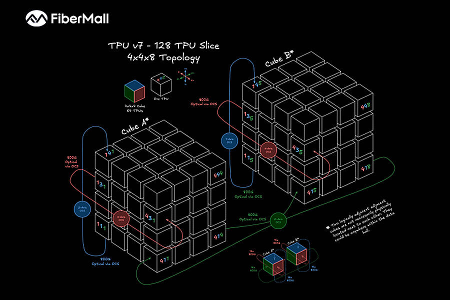
- (3) The scale-up memory domain:
- Pretraining demands the largest high-bandwidth domain to hold model, optimizer, and activations.
- A TPU pod ties thousands of chips into one domain via an OCS-reconfigured 3D-torus, optimized for pretraining collectives — in this area the ASIC's co-designed fabric matches or leads NVLink.
But this edge is narrow and conditional:
- It holds only for the few (Google, AWS, Meta) that (a) own stable, large workloads and (b) have the scale to amortize co-design capability and NRE (Non-Recurring Engineering).
- For the rest — where the model architecture changes fast (MoE variants, new attention, RL recipes) — the GPU's programmability is cheaper (ASICs have long respin cycles and cannot keep up).
▸ Designing a dedicated chip costs enormous one-time engineering (NRE). To recoup it you need a huge, stable workload of your own to run on it, which in practice limits it to the Google / AWS / Meta tier.
▸ Conversely, where the model structure changes often, the GPU's flexibility (programmability — you only edit code) wins — a dedicated chip takes 1–2 years to respin once built, so it cannot keep up with change.
And in the era — since o1-preview in September 2024 — where the line between inference and training (test-time compute) has blurred:
▸ It used to split into: training computes once and heavily at build time, inference computes lightly each time it is used.
▸ Since OpenAI's o1-preview in September 2024, the model reasons at length before answering (test-time compute), so inference too uses a lot of compute, and training came to resemble inference as the model generates its own attempts (rollouts) for reinforcement learning (RL). The compute character of training and inference blended into one.
- Here, "training" converges toward RL / reasoning post-training that generates rollouts (close to inference), while "inference" converges toward long reasoning chains (compute-heavy, close to training). In this blended phase:
- inference TCO is dominated by Nvidia (NVLink all-to-all for MoE + the CUDA / TensorRT-LLM ecosystem + the flexibility to absorb RL's frequent model changes),
- ▸ An MoE model sends each token to a different expert chip (different experts are stored on different GPUs) with a lot of send/receive communication (all-to-all),
- ▸ and NVLink, which links all GPUs directly to each other, is strong at this communication. Add CUDA / TensorRT-LLM (Nvidia's development and inference-optimization software) and the flexibility to run diverse models as-is.
- and the QAT + NVFP4 (FP4) combination
- Rubin's 5th-gen Tensor Core processes dense FP4 ~3.5x vs GB200, and
- QAT (quantization-aware training) trains models stably at FP4/FP8,
- so the low-precision edge applies to both training and inference at once.
- So as the inference/RL share grows, the training side too generally reverts to Nvidia GPU's TCO advantage.
- ▸ FP4 represents numbers in just 4 bits — a low-precision format. Lower precision lets the same chip do far more compute (Rubin's dedicated Tensor Core processes dense FP4 ~3.5x vs GB200), sharply cutting cost and power.
- ▸ The weakness is that low precision can break training — QAT (mimicking low precision from the start of training) prevents that. The low-precision format's benefit applies to both training and inference.
In sum,
- ASICs beat the GPU on perf/$ and perf/watt for the "stable pretraining you own" slice, but
- as the workload mix shifts toward reasoning / RL / inference and FP4 low precision, and for the majority who cannot co-design, Nvidia keeps the TCO crown — Apple's AFM 3 compute split (pretraining = TPU, largest-model serving = Nvidia) shows exactly this logic.
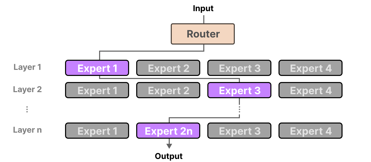
4.2 The Core Mechanism — Total Params in NAND, Routing at the Prompt Level
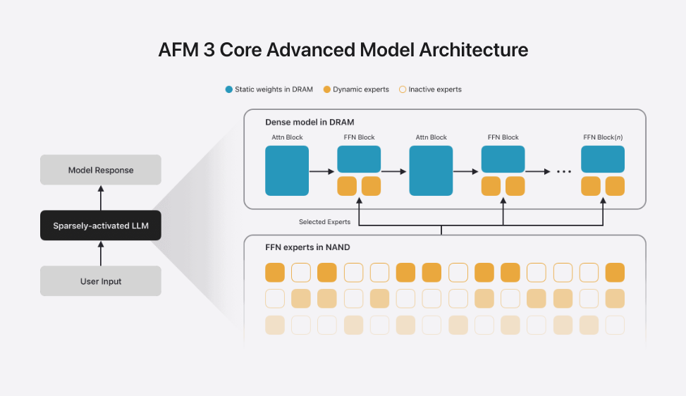
The core is the tiered memory placement of the MoE model:
- static weights (shared weights like attention) and active experts in DRAM,
- total params including inactive experts in NAND.
- From a memory-hierarchy view, because DRAM's $/GB is expensive, the parameter store is pushed one tier down (NAND) on the $/GB ↔ latency trade-off.
- But NAND-DRAM bandwidth is far too slow to swap experts per token as standard MoE does. So routing decisions are lifted all the way to the prompt level, deterministically designed to use a predetermined active-expert set per use case.
- In short, since randomness (random access from per-token routing) hits NAND's weakness, removing the randomness itself leaves only NAND's strengths ($/GB, capacity). Apple is a Tier 3 model by tier, but the attempt itself is interesting.
A parallel in design philosophy — both can be seen as the same family in that they cut runtime dynamism to sidestep the latency variance arising in the memory hierarchy.
- Groq's LP30 has the compiler fix compute and data movement at the cycle level and places the latency-sensitive working set in an SRAM-first structure, cutting the runtime jitter that comes from cache/HBM/DRAM dependence.
- Apple's AFM 3 Core Advanced defines MoE expert routing at the prompt level rather than the token level, refreshing the expert set only periodically when needed during answer generation. This keeps the whole model in NAND while loading only the expert sections actually needed into DRAM, distributing NAND↔DRAM weight movement.
That is, the shared point of both cases is "giving up the freedom of dynamic scheduling/routing in exchange for greater predictability in the memory hierarchy."
- The difference: Groq's structure uses faster static memory to guarantee latency predictability,
- whereas Apple's lowers the granularity of processing-path selection in order to use larger NAND flash as the base store.
4.3 Datacenter Cross-check — Applying NAND to the Inference Tier Is Already Underway
Apple's edge-side design is not an isolated experiment but the most radical version of a flow already underway in the datacenter — "inserting flash into the inference memory hierarchy."
Nvidia ICMS:
- A KV-cache-only tier ("G3.5") based on Ethernet-attached flash using BlueField-4 as the controller — in the hierarchy GPU HBM (T1) → Vera LPDDR5X (T2) → ICMS flash (T3.5) → general storage (T4), a structure that resides petabyte-scale KV cache in NAND.
- Similar to how Apple pushed model weights down to NAND, the datacenter is pushing context (KV cache) down to NAND.
SanDisk FY Q3'26 earnings call (4/30):
- "NAND flash is emerging as the only economically viable solution to deliver the capacity, performance, and efficiency required to keep models accessible for real-time inference at scale."
- KV cache / RAG demand low-latency flash for data "far beyond the model itself."
- Datacenter revenue +233% QoQ ($1.47B), eSSD reaching 25% of the portfolio, and the QLC-based Stargate SSD recognizing revenue from next quarter (FY Q4'26).
The place of HBF (High Bandwidth Flash):

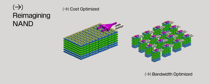
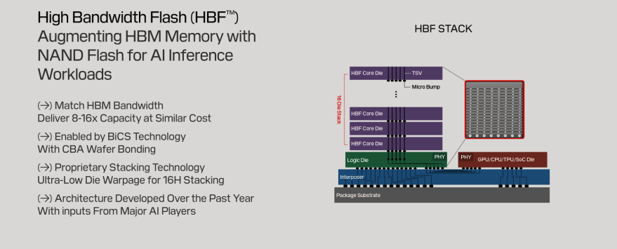
- On the SNDK call: "HBF is not a substitute for an enterprise SSD; it is a way to bring a lot more to inference in a different way."
- NAND die by year-end; the controller-inclusive system by early-to-mid next year.
- Combined with Mizuho's comments, HBF is not a component for today's AI systems but a technology that works only once the customer reshapes its model/hardware structure to fit HBF — so real revenue is expected to flow from CY28 onward.
- Apple AFM is precisely that first large-scale proof of "reshaping the model structure to fit flash" — showing that the co-design HBF-style architecture demands is actually feasible.
Micron (NASDAQ: MU) FY Q2'26 earnings call (3/18):
- "We are seeing an acceleration in NAND-based demand in the data center due to AI use cases such as vector database and KV cache offload."
- Volume production of G9-based PCIe Gen6 high-performance datacenter SSDs, spreading adoption of 122TB high-capacity SSDs, and in 2026 datacenter bits exceeding 50% of the DRAM+NAND industry TAM for the first time. NAND, like DRAM, is seen supply-constrained past 2026.
- Kioxia's Investor Day (§1) call for "AI-inference eSSD demand +86% per year" is the same context.
4.4 Implications
1 | The next step in memory-hierarchy restructuring.
- If the Moving Bits thesis (HBM demoted to cache, an optically-attached LPDDR pool as the main storage) is the datacenter's endpoint,
- Apple AFM shows that a configuration one step further down (DRAM → cache, NAND → main parameter store) already works at the edge. (Of course, for now this is an architecture applicable given Apple's Tier 3 model performance and the standardized usage pattern of Apple Intelligence within Apple's ecosystem. The key is that it was first to step up and show that "this is where it goes.")
- The common principle: the more access patterns are made deterministic and local, the cheaper the memory you can use as the main storage.
2 | A change in the character of NAND demand.
- Inference is pulling NAND up in two directions: (a) a KV-cache/RAG tier (ICMS, eSSD), (b) a parameter store (AFM, HBF).
- (a) is already showing in results (SNDK datacenter +233% QoQ, MU's acceleration comments),
- (b) is a CY28+ option. Both are consistent with the "context grows larger than the model" trend — structural demand created by reasoning / agentic workloads.
3 | MoE's sparse activation is flash-friendly.
- A dense model must stream all weights at every token-generation step, so NAND is impossible; but
- MoE only needs the active parameters in fast memory.
- How far a routing-frequency-lowering (prompt-level) variant preserves quality determines this architecture's scalability.
- Apple's use-case restriction (Siri, Apple Intelligence's repetitive, predictable prompt distribution) is the key premise.
4 | The beneficiary landscape.
- The order is eSSD mix expansion + QLC transition (SNDK Stargate, MU G9 QLC) → HBF-style co-designed flash (CY28+). With HBF's precondition — "the customer changing its model/HW structure" — proven by Apple, the next thing to watch is whether hyperscalers (especially the operators with the highest inference cost) make similar attempts.
Caveats:
- Apple AFM is Tier 3 on model quality, and prompt-level routing is a design suited to standardized OS-embedded use cases rather than free-form general-chatbot input. Generalizing to general-purpose datacenter MoE serving must verify the cost of routing-quality degradation.
- NAND's write-endurance / latency variance is mitigated under the read-heavy pattern of inference, but can become a constraint again if model-update (redeploy) frequency rises.
- The NAND-demand acceleration on the SNDK / MU calls mixes cyclical (supply constraint + price increase) and structural (inference tier) effects — the real test is whether only the structural effect remains when the cycle rolls over.
5. CPU — Agentic AI Creates a Third Demand Axis
5.1 The Three Classes of CPU Demand
1 | Host CPU / Headnode CPU
- The CPU directly attached to the GPU (e.g., a Vera Rubin Compute Tray has two sets of 1 Vera CPU + 2 Rubin GPUs).
- Its role: running GPU drivers, kernel launch, tokenization/staging, memory management, feeding data.
- What matters is per-core performance, GPU-CPU bandwidth, and memory capacity/bandwidth more than core count.
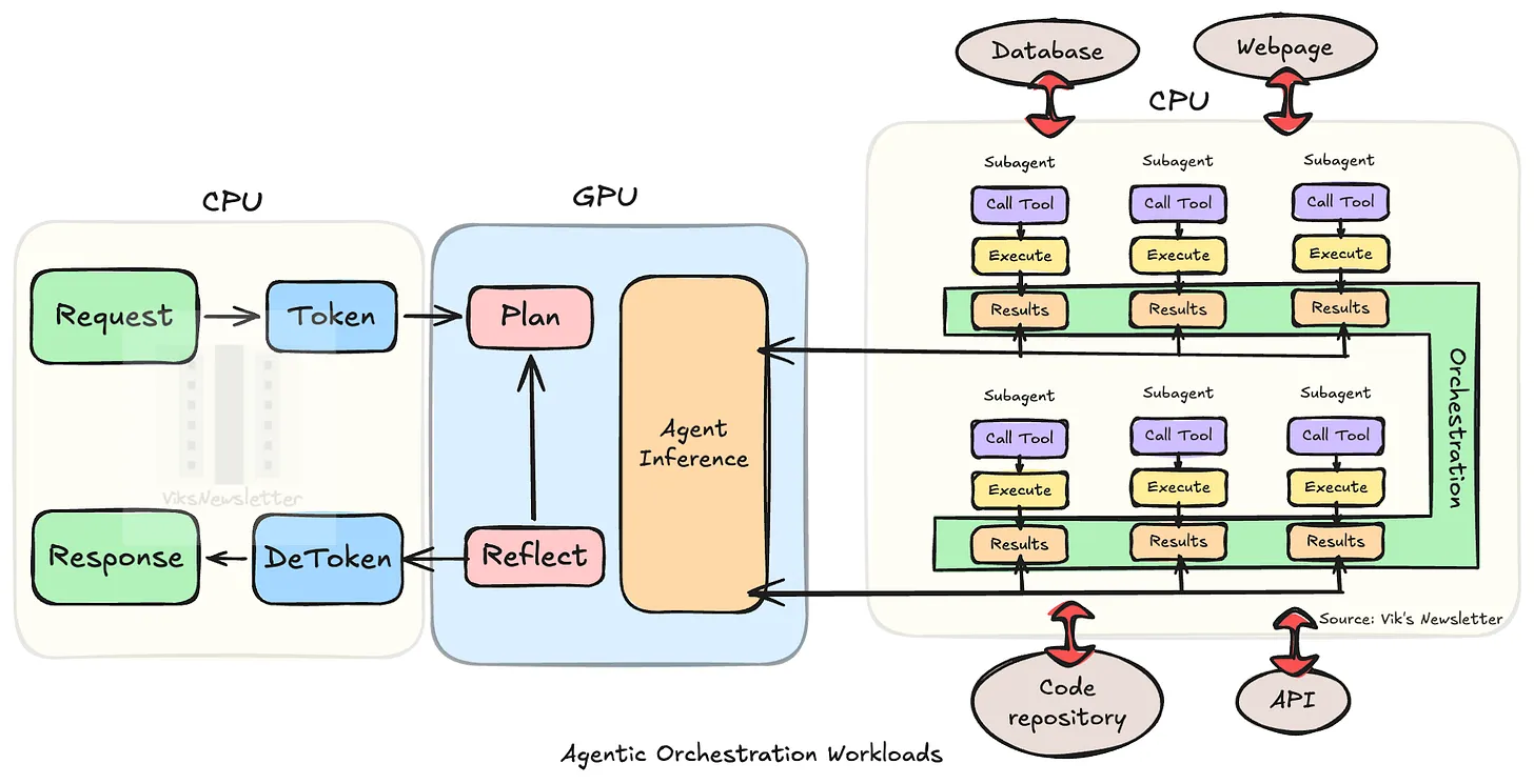
2 | Orchestration CPU (Standalone)
- A new workload created by Agentic AI.
- An agent asks the model → is instructed → runs software tools → asks again, repeatedly (GPU is the brain, CPU the hands and feet).
- Loading this on the host CPU bottlenecks GPU supply, so it is separated out.
- With hundreds-to-thousands of sub-agents now running in parallel, demand is on a one-way climb — the CPU share in the CPU:GPU ratio keeps rising.
3 | Traditional cloud-server CPU
- A mature market, fully segmented (general purpose / compute-, memory-, storage-optimized).
- Per-core licensing (SQL/VMware) prefers fewer cores + higher per-core spec; web prefers throughput/watt.
5.2 Why CPU TAM Is Expanding — Reasoning Changed the Workload
- In the past the GPU did not need much CPU memory (PCIe connection + a separate memory pool).
- Since reasoning arrived, tokens used per answer (context length) grew, KV cache exploded → GPU memory fills easily → the pattern of offloading KV cache to CPU DRAM and quickly reloading it became routine.
- From the Grace Blackwell generation Nvidia made the GPU use CPU memory as its own via NVLink-C2C (PCIe one-way 128GB/s → 900GB/s), set to widen to 1.8TB/s on Vera.
- So NVLink's moat is twofold:
- (a) the all-to-all nature of the switched scale-up network meshes with MoE communication, giving overwhelming performance vs inference TCO,
- (b) thanks to C2C, the bottleneck of KV-cache movement between GPU ↔ host CPU is small.
- The external opening of NVLink Fusion is a swing factor: AWS adopts it from Trainium 4 — whether Nvidia gets to sell host CPUs into Trainium 4 systems too is the thing to watch.
5.3 The TAM Frame — Agentic CPU More Than 2x Traditional Cloud CPU
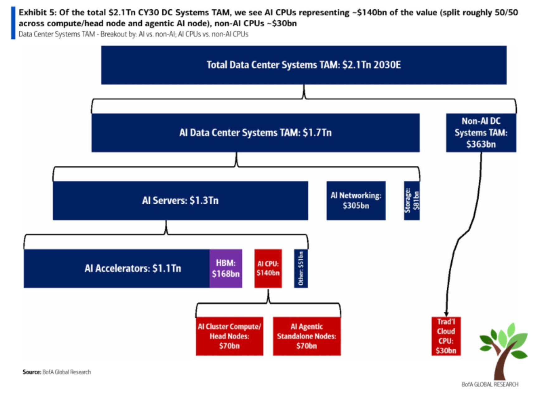
- BofA's CY30E breakdown: AI CPU $140B (head node $70B + agentic standalone $70B) vs traditional cloud CPU $30B — agentic alone is more than 2x the traditional-cloud-CPU TAM, and AI CPU in total is ~4.7x.
- Implication: the conventional wisdom that "CPU is a mature market" no longer holds, given the emergence of classes 1 and 2. This is the backdrop for CPU names trading at CY27 P/E 30+ (the same structure as the re-rating logic of §1).
5.4 This Week's Verification Point — the SOCAMM2 Spec Change Is Not a Downgrade but a Q Increase
"Nvidia's SOCAMM2 demand has risen 10–20% recently"
- The module's main spec changed from 192GB → 96GB, which on the surface looked like a down-spec, but in reality 192GB configs −50% / 96GB configs +400% / 64GB +50% raised total module shipments — Nvidia's total LPDDR5X bit demand is actually +10–20%.
- The capacity/BOM/rack-price changes (1.5TB → 768GB, BOM 21.4% → 12.2%, rack price $7.6M → $6.8M, −10.5%) were already covered in §1.1 — the customer price cut is small, but Nvidia gets to sell more systems on the same memory budget plus higher-margin GPU/networking content (dollar content rises).
- What matters is that the background of the capacity cut is itself that the Vera CPU's competitiveness is higher than expected, prompting a reallocation.
- And by laying down more NVL72 / CPU racks / STX racks ahead of time (higher Q), there remains live demand to upgrade SOCAMM2 to high-capacity modules later as the agentic-AI workload share rises — an event that opens medium-to-long-term memory upside.
By player:
- Memory: reconfirmed tightness from finished-goods demand pull + an upgrade option.
- Optical / SOCAMM2 value chain (same substrate, materials, back-end): the benefit of rising rack Q flows straight through.
This Week, In Sum
- Memory & storage:
- LTA proliferation (SNDK 80% minimum GPM) + finished-goods demand pull + HDD pricing power,
- the conditions for a cyclical → secular re-rating are piling up.
- Optics:
- the scale-up CPO "delay" is not new,
- scale-out, OCS, and scale-across were all upward in tone at the earnings-call level.
- The common bottleneck is InP capacity, and from this week the region of InP sourcing (China vs Japan vs in-house or diversified) is a new axis of differentiation.
- Power & datacenter:
- the real bottleneck is not the turbine factory but the EPC system (labor +30% YoY, NIMBY).
- That bottleneck structure is pushing the mix toward prefabricated, lead-time-reliable generation (SOFC) — the Wyoming customer swap (Oracle → Google) leaving SOFC volume unchanged is the proof.
- Apple AFM 3:
- the first large-scale proof of NAND-based MoE inference,
- edge-side confirmation of the structural flow of NAND's promotion into the inference tier (KV cache → parameter store).
- CPU:
- agentic workloads promote the CPU to a third demand axis (BofA CY30E AI CPU $140B vs traditional cloud $30B).
- the reality behind the SOCAMM2 "spec down" reports is a Q increase of +10–20% bit demand.